Intel's 10nm Cannon Lake and Core i3-8121U Deep Dive Review
by Ian Cutress on January 25, 2019 10:30 AM ESTFrequency Analysis: Cutting Back on AVX2 vs Kaby Lake
Analyzing a new CPU family as a mobile chip is relatively difficult. Here we have a platform that is very much hamstrung by its thermal settings and limitations. Not only that, the BIOS adjustments available for mobile platforms are woeful in comparison to what we can test on desktop. This applies to the Intel NUC that came to retail in December as well as the Lenovo Ideapad E330-15ICN that we have for testing.
The issue is that for a 15W processor, even when built in a ’35 W’ capable environment, might still hit thermal limits depending on the configuration. We’ve covered why Intel’s TDP often bares little relation to power consumption, and it comes down to the different power levels that a system defines. It can also depend a lot on how the chip performs – most processors have a range of valid voltage/power curves which are suitable for that level of performance, and users could by chance either get a really good chip that stays cool, or a bad chip that rides the thermal limits. Ideally we would have all comparison chips in a desktop-like environment, such as when we tested the ‘Customer Reference Board’ version of Broadwell, which came in a desktop-like design. Instead, we have to attach as big of a cooling system as we can, along with extra fans, just in case. Otherwise potential variations can affect performance.
For our testing, we chose Intel’s Core i3-8130U mobile processor as the nearest competition. This is a Kaby Lake dual core processor, which despite the higher number in its name is using the older 14nm process and older Kaby Lake microarchitecture. This processor is a 15W part, like our Cannon Lake Core i3-8121U, with the same base frequency, but with a slightly higher turbo frequency. Ultimately this means that this older 14nm processor, on paper, should be more efficient than Intel’s latest 10nm process. Add on to this, the Core i3-8130U has active integrated graphics, while the Cannon Lake CPU does not.
Because both CPUs have turbo modes, it’s important to characterize the frequencies during testing. Here are the specifications and turbo tables for each processor:
| Comparing Cannon Lake to Kaby Lake | |||||
| 10m Cannon Lake Core i3-8121U |
AnandTech | 14nm Kaby Lake Core i3-8130U |
|||
| 2 / 4 | Cores / Threads | 2 / 4 | |||
| 15 W | Rated TDP | 15 W | |||
| 2.2 GHz | Base Frequency | 2.2 GHz | |||
| 3.2 GHz | Single Core Turbo | 3.4 GHz | |||
| 3.1 GHz | Dual Core Turbo | 3.4 GHz | |||
| 2.2 GHz | AVX2 Frequency | 2.8 GHz | |||
| 1.8 GHz | AVX512 Frequency | - | |||
The Cannon Lake processor loses frequency as the cores are loaded, and severely loses frequency when AVX2/AVX512 is applied based on our testing. Comparing that to the Kaby Lake on Intel’s mature 14nm node, it keeps its turbo and only loses a few hundred MHz with AVX2. This part does not have AVX512, which is a one up for the Cannon Lake.
The biggest discrepancy we observed for AVX2 was in our POV-Ray test.
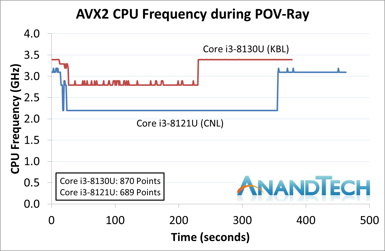
Here the Kaby Lake processor sustains a much higher AVX2 frequency, and completes the test quicker for a 26% better performance. This doesn’t affect every test as we’ll see in the next few pages, and for AVX-512 capable tests, the Cannon Lake goes above and beyond, despite the low AVX-512 frequency. For example, at 2.2 GHz, the Kaby Lake chip scores 615 in our 3DPM test in AVX2 mode, whereas the Cannon Lake chip scores 3846 in AVX512 mode, over 6x higher.
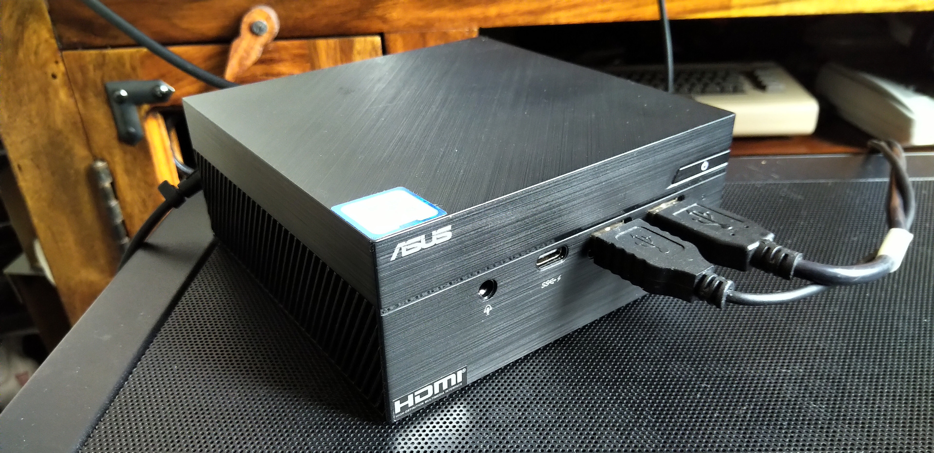
The system we are using for the Core i3-8130 is ASUS’ PN60 Mini-PC. This device is an ultra-compact mini-PC that measures 11.5mm square and under 5cm tall. It is just big enough for me to install our standard Crucial MX200 1TB SSD and 2x4GB of G.Skill DDR4-2400 SO-DIMMs.
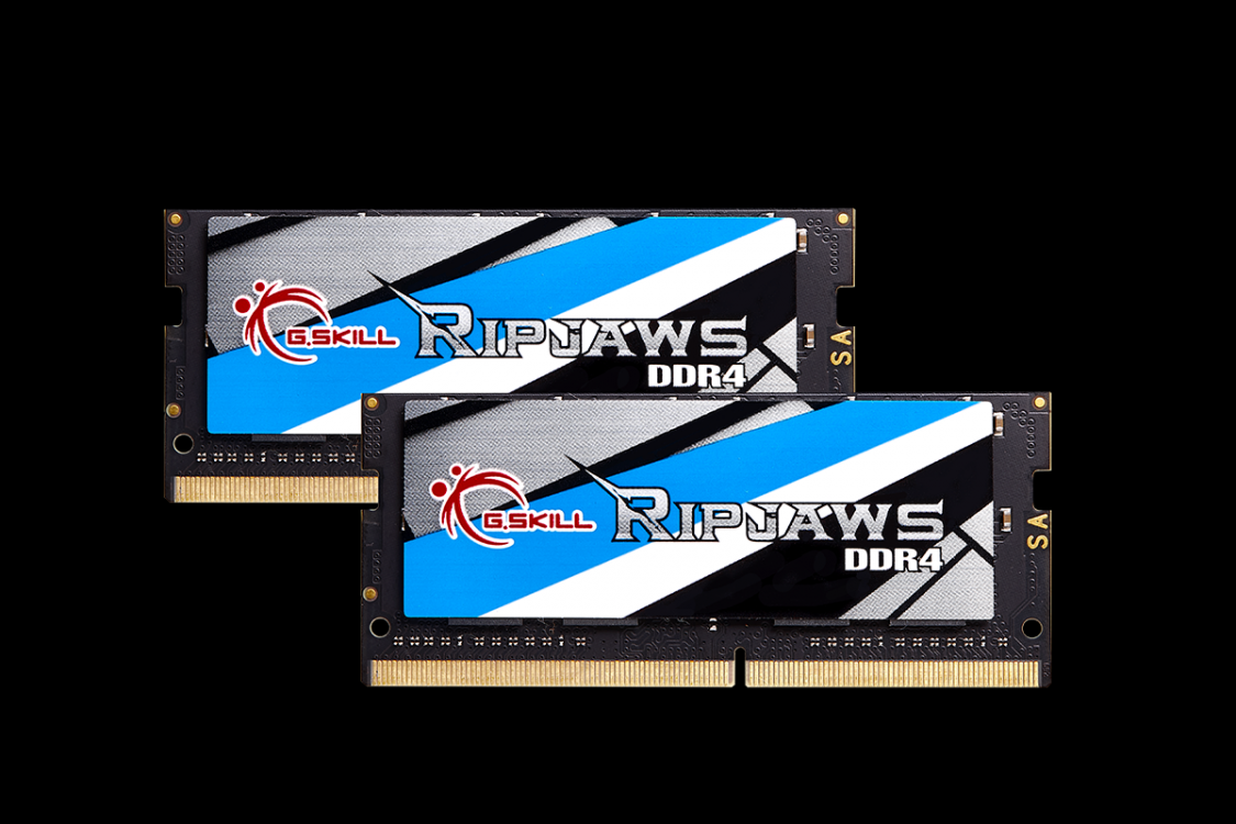
For the Cannon Lake based Lenovo Ideapad 330-15ICN, we removed the low-end SSD and HDD that was shipped with the design and put in our own Crucial MX200 1TB and 2x4 GB DDR4 SO-DIMMs for testing. Unfortunately we can’t probe the exact frequency the memory seems to be running at, nor the sub-timings, because of the nature of the system. However the default SPD of the modules is DDR4-2400 17-17-17.


129 Comments
View All Comments
jjj - Friday, January 25, 2019 - link
Bored with laptops, want a large foldable phone with a projected keyboard so i can forget about these bulky heavy things. Ok, fair enough, glasses are way better but those will take a while longer.eastcoast_pete - Friday, January 25, 2019 - link
@Ian: Thanks for the deep dive, and giving the references for background! One comment, three questions (they're related): In addition to being very (overly) ambitious with the 10 nm process, I was particularly struck by the "fused-off integrated graphics" and how Intel's current 10 nm process apparently just won't play nice with the demands in a GPU setting. Question: Any information or rumors on whether that contributed to AMD going the chiplet route for Ryzen going forward? In addition to improving yields, that also allows for heterogeneous manufacturing nodes on the same final chip, so that can get around that problem. Finally, any signs that Intel may go down that road in its upcoming mainstream chips? Any updates on what node they will make their much-announced dGPUs on? Probably won't be this or a related 10 nm process.Lastly, and maybe you and Andrei can weigh in on that: TSMC's (different) 7 nm process seems to work okay for the (smaller) different "iGPUs" in Apple's 12/12x, Huawei's newest Kirin and the new Snapdragon. Any insight/speculation which steps of Intel's 10 nm process cause the apparent incompatibility with GPU usage scenarios?
Thanks!
Rudde - Saturday, January 26, 2019 - link
AMD has lauched huge 7nm desktop graphics cards (2 server and Radeon VII). AMD does not seem to have any problems making gpus on TSMC 7nm.eastcoast_pete - Sunday, January 27, 2019 - link
That's why I asked about the apparent incompatibility of GPU-type dies with Intel's 10 nm process. Isn't it curious that this seems to be the Achilles heel of Intel's process? I wonder if their future chips with " iGPU" will use a chiplet-type approach, with the CPU parts in 10 nm, and the GPU in 14 nm++++ or however many + generations it'd be on. The other big question is what process their upcoming high-end dGPU will be in Unless, Intel let's TSMC make that for them, too.velanapontinha - Friday, January 25, 2019 - link
Every time I read Kaby G I'm instantly stormed by a Kenny G theme stuck in my head, and it ruins the rest of my day.Please stop.
skis4hire - Friday, January 25, 2019 - link
"Fast forward several months later, to May 2018, and we still had not heard anything from Intel."Anton covered their statement in April, where they indicated they weren't shipping volume 10nm until sometime in 2019, and that they would instead release another 14nm product, whiskey lake, in the interim.
https://www.anandtech.com/show/12693/intel-delays-...
Yorgos - Friday, January 25, 2019 - link
>AMD XXXXX (XM/XT, XXW)Thanks Ian for reminding us is every article, that we are reading a Purch media product, or a clueless editor.
Don't forget, 386 was o 0 core CPU.
No, it doesn't bother me as a reader, it bothers me as an engineer who designs and studies digital circuits. But hey you can't have it all, it's hard to find someone who is capable at running windows executables AND know his way in comp. arch..
Ryan Smith - Friday, January 25, 2019 - link
While I'm all for constructive feedback, I have to admit I'm not sure what we're meant to be taking from this.Could you please articulate in more detail what exactly is wrong with the article?
KateH - Saturday, January 26, 2019 - link
i interpreted it as,...
"I disagree with the distinction between 'modules' and 'cores' that is made when some journalistic endevours mention AMD's 'Construction' architecture microprocessors. I find the drawing of a line based on FPU counts inaccurate- disengenous even- given that historic microprocessors such as the renowned Intel 80386 did not feature an on-chip FPU at all, an omission that would under the definitions used by this journalist in this article cause the '386 to be described as having 'zero cores'. The philosophical exercise suggested by such a definition is, based upon my extensive experience in the industry of digital circuit design, repugnant to my sensibilities and in my opinion calls into question the journalistic integrity of this very publication!"
...
or something like that
(automatically translated from Internet Hooligan to American English, tap here to rate translation)
Ryan Smith - Saturday, January 26, 2019 - link
"tap here to rate translation"5/5 stars. Thank you!