Intel's 10nm Cannon Lake and Core i3-8121U Deep Dive Review
by Ian Cutress on January 25, 2019 10:30 AM ESTIntel’s Path to 10nm: 2010 to 2019
The manufacturing history from Intel has been a very successful one. Being vertically integrated has meant that it can save costs, but also tailor its manufacturing processes to exactly what it needs without relying on an external company to do the tweaking. Since as far back as 2005 and the 65nm process, Intel embarked on a strategy of ‘Tick-Tock’, meaning that on alternate generations of products the company would release either a new process technology or a new processor microarchitecture. This allowed Intel to either reap the benefits of a faster processor design in the new microarchitecture, or reap the benefits of a smaller process node allowing for lower voltage, lower power, and smaller transistors to add in new features.
| Intel's Core Architecture Cadence | |||||
| Core Generation | Microarchitecture | Process Node | Release Year | ||
| 2nd | Sandy Bridge | 32nm | 2011 | ||
| 3rd | Ivy Bridge | 22nm | 2012 | ||
| 4th | Haswell | 22nm | 2013 | ||
| 5th | Broadwell | 14nm | 2014 | ||
| 6th | Skylake | 14nm | 2015 | ||
| 7th | Kaby Lake | 14nm+ | 2016 | ||
| 8th | Kaby Lake Refresh Coffee Lake Cannon Lake |
14nm+ 14nm++ 10nm |
2017 2017 2017* |
||
| 9th | Coffee Lake Refresh | 14nm++ | 2018 | ||
| Unknown | Ice Lake (Consumer) | 10nm class | 2019 | ||
| Cascade Lake (Server) Cooper Lake (Server) Ice Lake (Server) |
14nm class 14nm class 10nm class |
2019 2019? 2020 |
|||
| * Single CPU For Revenue ** Intel '14nm Class' is the new designation, moving away from '+' |
|||||
During this time, Intel held its annual Intel Developer Forum conference, known as IDF. IDF was a great show for the company to showcase its latest and greatest, as well as talk about what the future holds. It also allowed journalists and developers to discover the interesting technological advantages and platforms that Intel had built in order to accelerate computer code and projects. Being able to fully use the extra performance or extra power each generation enabled the product stack to be taken up to its zenith, as well as discuss future product lines and features.
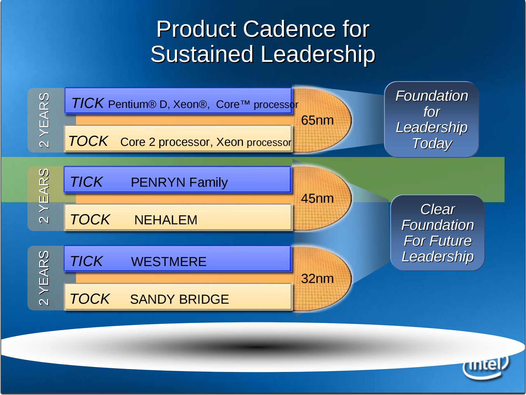
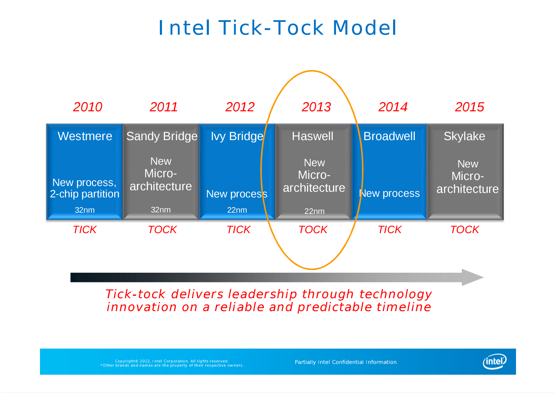
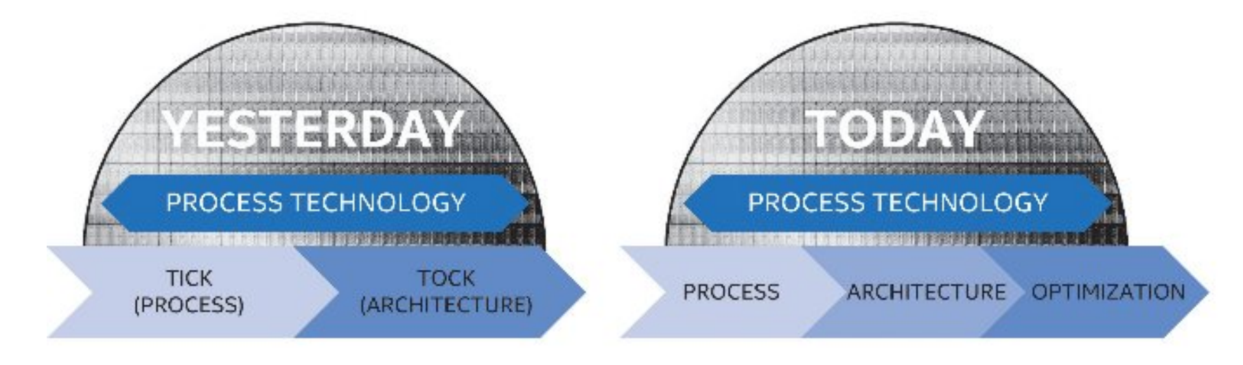
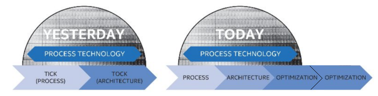
As this image shows, each combination ‘Tick-Tock’ was designed to be around two years apiece. Ticks were new process nodes, and Tocks were new microarchitecture. One of the famous comments of the era was the phrase ‘real men don’t tick tock, they tock tock tock’ (implying that microarchitecture improvements were more important in the long run than new process nodes).
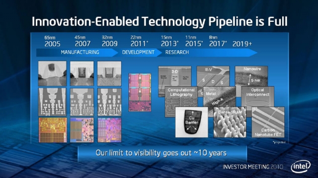
It is worth noting that Intel typically quotes that their development and research model goes to the next ten years of products, offering visibility and implementations that might cause the next paradigm of computing. Here, in this 2010 Investor Meeting slide, we see that Intel had 22nm in development for 2011, and was expecting ‘15nm’ to hit in 2013, ’11 nm’ for 2015, and ‘8nm’ for 2017. These names are different to the 14nm, 10nm, and 7nm we call them today, likely due to an International Technology Roadmap for Semiconductors (ITRS) report which originally had these nodes listed as 15, 11, and 8. It very quickly changed into the following slide:
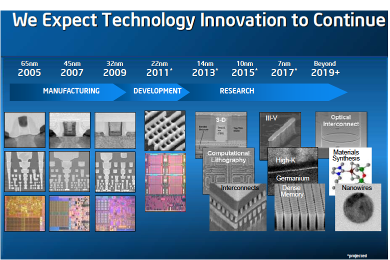
Here we see some of what Intel was working on: 3D transistors, computational lithography, interconnects, III-V materials, High-K metal gates with Germanium, Dense SRAM, Optical Interconnects, Material Synthesis, and Nanowires. Some, all, or fewer of these projects are still in play today in 2019.
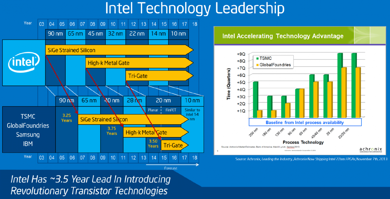
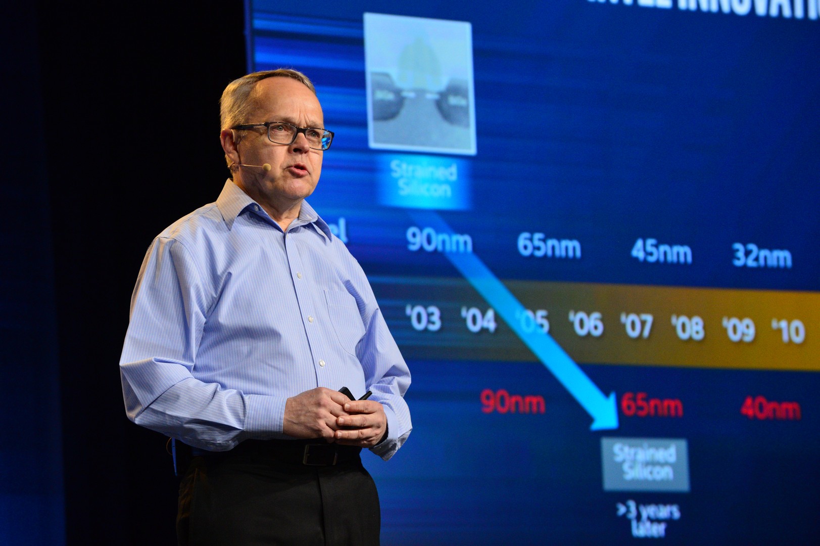
Intel has often used these technologies as a marker for its industry prowess against the foundry players in the marketplace, such as TSMC, GlobalFoundries, and Samsung. In this slide from 2014, we see Intel showing that it had a 3.25-year lead against others in Silicon-Germanium strained silicon, a 3.75-year lead in High-K metal gate technology, and a 3.5-year lead to tri-gate transistors, as well as the transition to FinFETs. Intel introduced FinFETs at 22nm, whereas the rest of the industry had them at 16nm.
It’s worth noting that on this 2014 diagram, Intel has 14nm listed as a 2014 technology, while 10nm is listed as a 2016 technology.
From 2010 onwards, Intel introduced the Core brand for its microarchitecture, which is still prevalent today (although with many generations of enhancements). At around 2012, Intel still expected to remain on Tick-Tock for several years at a minimum, moving from 32nm to 22nm, then to 14nm and 10nm. Unfortunately, Intel experienced delays bringing 14nm to market.
Despite originally being a product for 2013, the yields on 14nm fell short of targets, and compared to 22nm, it was clear that the jump to the next generation of FinFETs with a combination of density increases, active power decreases, and performance per watt increases was harder and harder to achieve. At this point in November 2013, Intel was expecting to match the yield of 22nm in Q1. However 14nm wasn’t just delayed into the beginning of 2014.
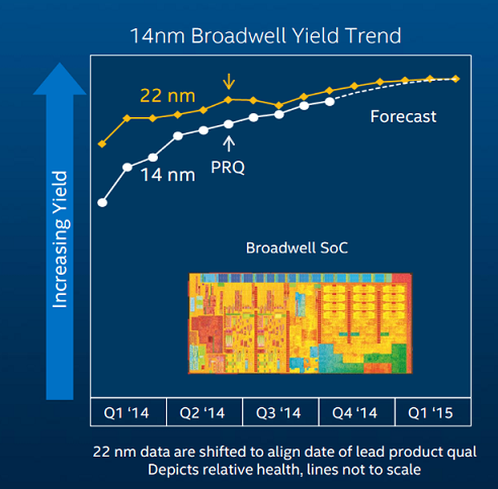
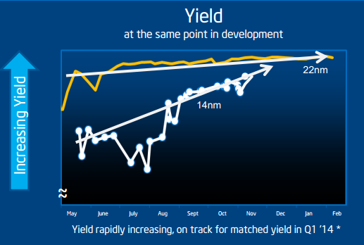
In mid-2014, Intel published this graph showing that even with expected advances, they weren’t going to match 22nm yields into 2015. However the key point here is the PRQ date, or Production Release Qualification date, meaning that Intel was sufficiently happy that yields were high enough and the performance was suitable for silicon to be made for retail products. Intel gave a deep dive into its 14nm technology in August 2014, and Ryan did a great write up here. The detail is key – it is genuinely possible to see why 14nm was so much harder than 22nm.
The first products on 14nm were the smallest designs for the ‘Broadwell-Y’ family of processors. These 4.5W processors were marketed to enable thinner and lighter form factor mobile devices, due to the decreased power consumption of the new process. Ultimately, these chips were easier to manufacture (yield decreases with an increase in chip size) as well, allowing Intel to start selling processors despite a higher-than-expected defect rate. These processors were officially on the market in the September/October 2014 timeframe.

Ultimately it was 2015 when we saw something bigger from Intel’s 14nm process. In Q1, we saw a launch of mid-range laptop and notebook processors on this first generation 14nm process, with higher performance Core i7 processors in June 2015. Intel did actually launch a couple of desktop processors as part of this Broadwell family, the Core i7-5775R and the Core i5-7675R, in June 2015 however they were not widely available and short lived. The far more successful second generation of 14nm processors, Skylake, was launched on the desktop in August 2015 with a couple of high-end parts, followed by the rest of the stack in Q3/Q4 of that year.
Speaking to some in the industry, one of the main reasons why Intel had so much trouble with Broadwell and its first generation 14nm process was related to its integrated graphics. Reports suggested that Intel’s high-performance transistors on 14nm were not suited to the high-frequency design of the newest graphics libraries, with one report stating that Intel had promised a certain level of graphics performance and wasn’t able to achieve it, ultimately leading to a launched product with lower graphics performance than expected. Over time Intel has improved its 14nm process to get that frequency back (it took a couple more generations), although this will play into our discussions on 10nm as well.
In 2015, this was Intel’s official roadmap:
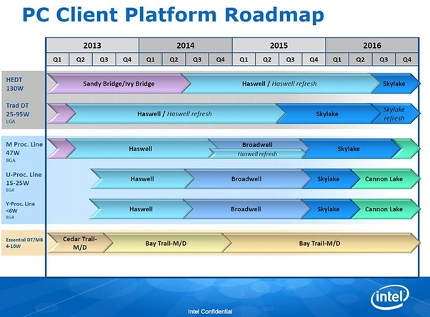
Here we see the late 2014 launch of 14nm Broadwell for the mobile processors, and the complete rejection that Broadwell for the traditional desktop even existed, going straight into the second generation of 14nm with Skylake in Q2 2015. At this point I want to draw attention to the bits in green. Under Intel’s Tick Tock process, the first generation 10nm process, Cannon Lake, was set to follow Skylake very quickly with a launch in Q2 2016.
If Intel was aiming at Q2 2016 for 10nm products to be on shelves, it would have seemed very reasonable at the time, given that at the start of 2015, Intel had its usual array of discussions and presentations at the International Solid-State Circuits Conference (ISSCC) in February. As part of those presentations, 10nm was a key part of it, with Intel stating that while 10nm was set to have more masking layers than 14nm, the company expected that the delays that bogged down 14nm would not be present in bringing 10nm to market. We specifically reported at the time:
In this, the key part is that Intel had identified where it went wrong in 14nm, and was ready to remove those bottlenecks in its development of 10nm. Intel stated that 10nm would come with innovation, however going beyond to 7nm will require new materials and processes that Intel would introduce progressively. After ISSCC, Skylake on 14nm was launched in mid-to-late 2015.
In a report by Intel in March 2016, it was clear that 10nm Cannon Lake was not ready. The company released the following statement in its annual 10-K filing:
What this means is that Intel was extending its product cycle for 14nm. Intel’s famous Tick-Tock cadence, which had served them well for several cycles, was now being split into a ‘Process Architecture Optimization’ strategy. Under this heading, Intel would release three versions of processors under a given process node: one focused on transitioning to the new process, one to introduce a new microarchitecture, and one to optimize both the process and the architecture.
For roadmaps and product lines, this meant that the second generation of 14nm called Skylake would transition into the third generation of 14nm, called Kaby Lake. Officially this process optimization was dubbed ‘14nm+’, with the plus indicating it had a little bit extra. Explicitly, the new process had improved transistor channel strain along with other minor enhancements that enabled Intel to extract 100-300 MHz more out of the design without increasing the capacitance. The overall improvement allowed for an additional +12% drive current, leading to increased performance.

Kaby Lake was officially launched in August 2016, starting with the 4.5W parts again, with the desktop processors coming in January 2017.
To kick of 2017, at CES, Intel held a presentation focused on VR. At some point towards the end, the CEO held up a 2-in-1 laptop that he said was 10nm. It was for all accounts the first presentation of 10nm we had seen. Nothing was run on the device, and the device was held up for only a few brief seconds.
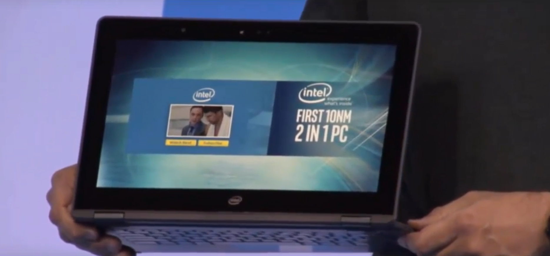
This happened within the first two minutes of the presentation, with the former CEO Brian Krzanich stating categorically that Intel would be shipping 10nm by the end of the year.
Soon after at an Intel Investor Day in February 2017, Intel dropped a bombshell about its product portfolio for the upcoming year. The company announced that the data center would be first to new process nodes (later clarified to mean 10nm+), and that it would be taking another swing at 14nm for its consumer product lines. Within one generation of products, Intel’s ‘Process-Architecture-Optimization’ was given a double dose of the Optimization.
This would mark the fourth generation of 14nm products for Intel, which ended up being called Coffee Lake, and was formally launched in May 2017. This fourth generation of 14nm was even given the process labelling of ‘14nm++’, following Broadwell (14nm), Skylake (14nm), and Kaby Lake (14nm+). We were still waiting on news for the first generation of 10nm, Cannon Lake, would have been expected to debut in mobile processors first. Remember, the original predicted date of 10nm was 2015, so at this point Intel is two years late.
After the Investor Day in February 2017, the company had its first Intel Manufacturing Day at the end of March 2017. The company went into more detail about its 10nm plans, and specifically regarding some of the new technology designs integrated into its 10nm process. Presentations were made by Stacy Smith, the then CTO, Mark Bohr, Dr. Murthy Renduchintala, Ruth Brain, and Kaizad Mistry, with a focus on Intel’s latest technology and foundry processes.
Mark Bohr’s Presentation on Moore’s Law
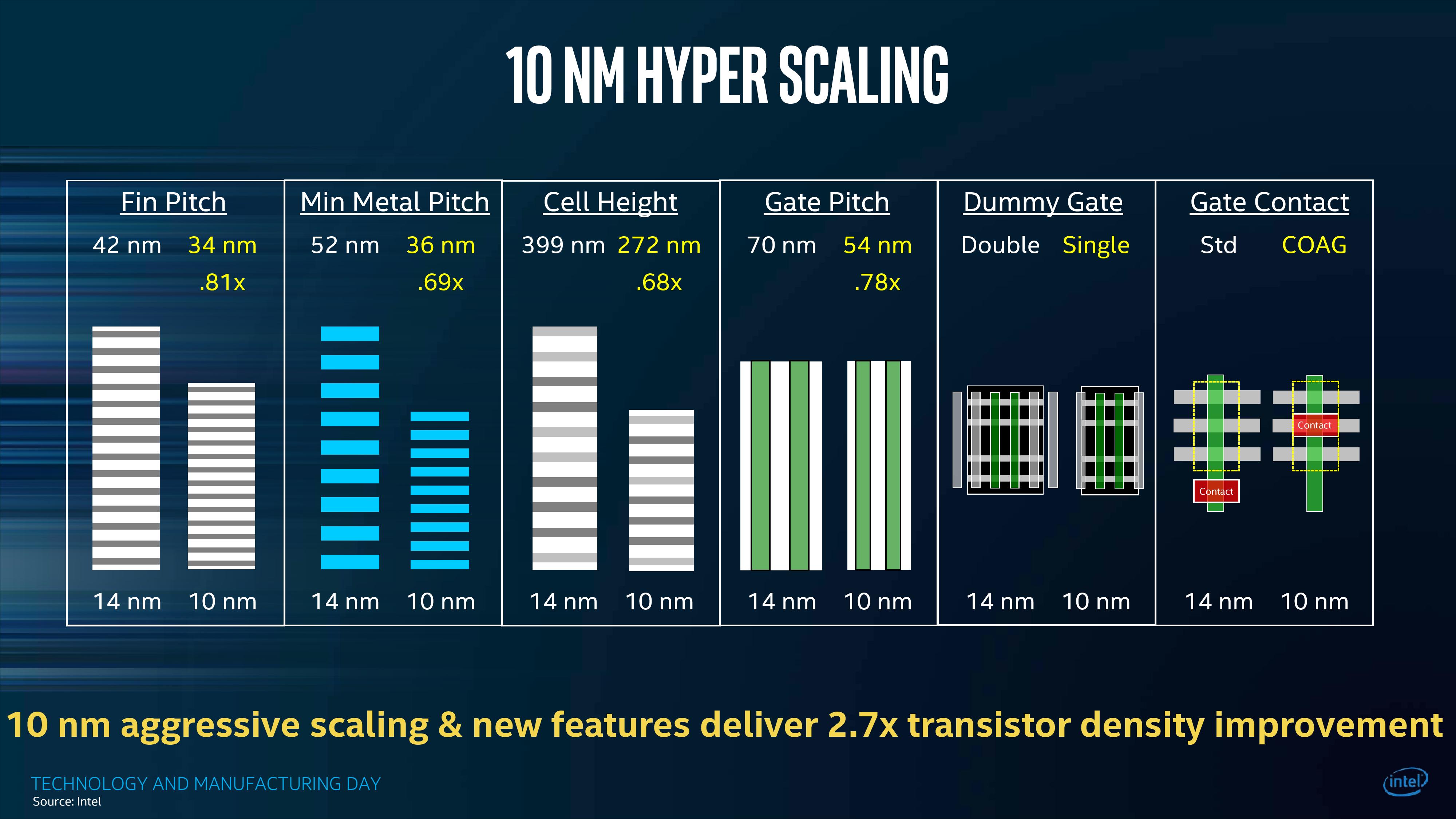
We’ll go into more details about the specifics on 10nm in the next page, however the Manufacturing Day was very well received by media and analysts alike. The company explained that it was focusing on transistor density improvement, showing improvements in fin pitch, metal pitch, cell height, and gate pitch, as well as new technologies such as single dummy gates and Contact Over Active Gate (COAG). The key takeaway is that Intel was aiming for 100 million transistors per square millimeter with its 10nm process, and this would allow it to keep its 3.5 year lead over other foundry offerings, with Intel predicting that their own 10nm offering would be better than TSMC/GF/Samsung’s 7nm. Some in the media were blown away with the numbers, others were not so easily impressed, pointing out Intel’s wordiness to make some of the numbers work.
Another takeaway is that after not saying much about 10nm for a while, Intel was opening up. However, the company very quickly became quiet again.
After manufacturing day, we saw the launch of Coffee Lake, but the next update on 10nm was given in mid-August, where Intel announced the name of the second generation of 10nm: Ice Lake.
As mentioned at the time, announcing the name of the n+2 processor family seemed a little odd, especially given the first 10nm generation had been delayed at least twice already and had not been released. It would later become evident, in mid-2018, that the Ice Lake naming was pushed out due to its use in the first generation of 10nm for Intel’s Xeon server line of products.
In September, Intel re-ran its Manufacturing Day event in Beijing, again discussing its lead in process technology and the upcoming 10nm ‘revolution’. Nothing new was said at the event, except that a 10nm wafer was shown on stage and in the breakout sessions for the event.
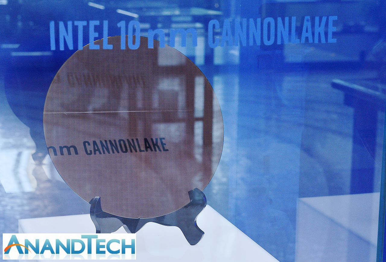
Based on this wafer, we estimated that the 2+2 (dual core with GT2 graphics) configuration for a chip (which this wafer was built on) would be around 70.5 mm2 of die area. It turns out this was a pretty accurate estimation. Nonetheless, the pattern was set: we should expect to see 10nm in a 2+2 configuration coming to market as the first 10nm chip. At this point, we’re still expecting Intel’s Cannon Lake to be part of a full family of products.
After September, Intel went into radio silence mode again. The rest of 2017 came and went, with not much of a peep from the company. December came and went, and aside for an update on parts of the 10nm design at the IEDM conference, not a word came from outside Intel’s R&D efforts, with the company seemingly missing its own target of shipping 10nm in 2017. In early January is the annual industry CES trade show, where Intel had a keynote presentation, so we perhaps might hear something then.
Intel’s CES 2018 Keynote presentation, led by former CEO Brian Krzanich, was all pomp and ceremony. There was a mention of the recent Spectre and Meltdown security issues that were just announced, but the event focused on Intel enabling customers, as well as flashy drones, 3D volumetric video, AI, and LEDs.

In the presentation, Intel’s work in both neuromorphic computing and quantum computing was mentioned, along with showing a quantum chip on stage. However nothing relating to the next generation of general purpose computing processors was mentioned. AT ALL. Despite the CEO making the proclamation at CES 2017 of shipping by the end of the year, he didn’t even address the topic in the entire keynote in 2018. Something was afoot. We had a few words with our Intel spokespeople, who told us to be at the Intel booth at 8am the next morning for a small presentation.
In that small presentation, Gregory Bryant, SVP of the Client Computing Group, spent 10 minutes discussing how Intel was achieving its goals to bring the best computing experiences to its users. It was, in all honesty, a lot of fluff. Then in the final sentence of the ten minute presentation, he stated an update on 10nm, that the company had shipped product in 2017 for revenue. Then the presentation ended – no elaboration of what, or scope, or customer, or anything. It was a certain attempt to both mention 10nm at the show and not mention it all at the same time.

SVP Gregory Bryant mentioning 10nm, briefly
We all thought this was a bit odd. We knew that Cannon Lake was a consumer product, so this wasn’t a case of Intel shipping a server processor to top customers before announcing it (a common practice). But Intel at this point had given us very little details about the configurations, the performance, the pricing. For a company that takes pride on its engineering prowess, this was about as low-key of an announcement as you could get. We were very skeptical indeed.
The next mention of Cannon Lake was during February 2018, when Intel accidentally exposed in official documents that it had updated its microcode for two Cannon Lake processors. This update was to mitigate against certain Spectre and Meltdown vulnerabilities, confirming in a way that the hardware design for this family of processors was complete.
Also in 2018, Intel once again presented 10nm at the ISSCC conference in February. The focus of this talk ended up being once again about density, in this case the SRAM cells which showed a 0.63x scaling.
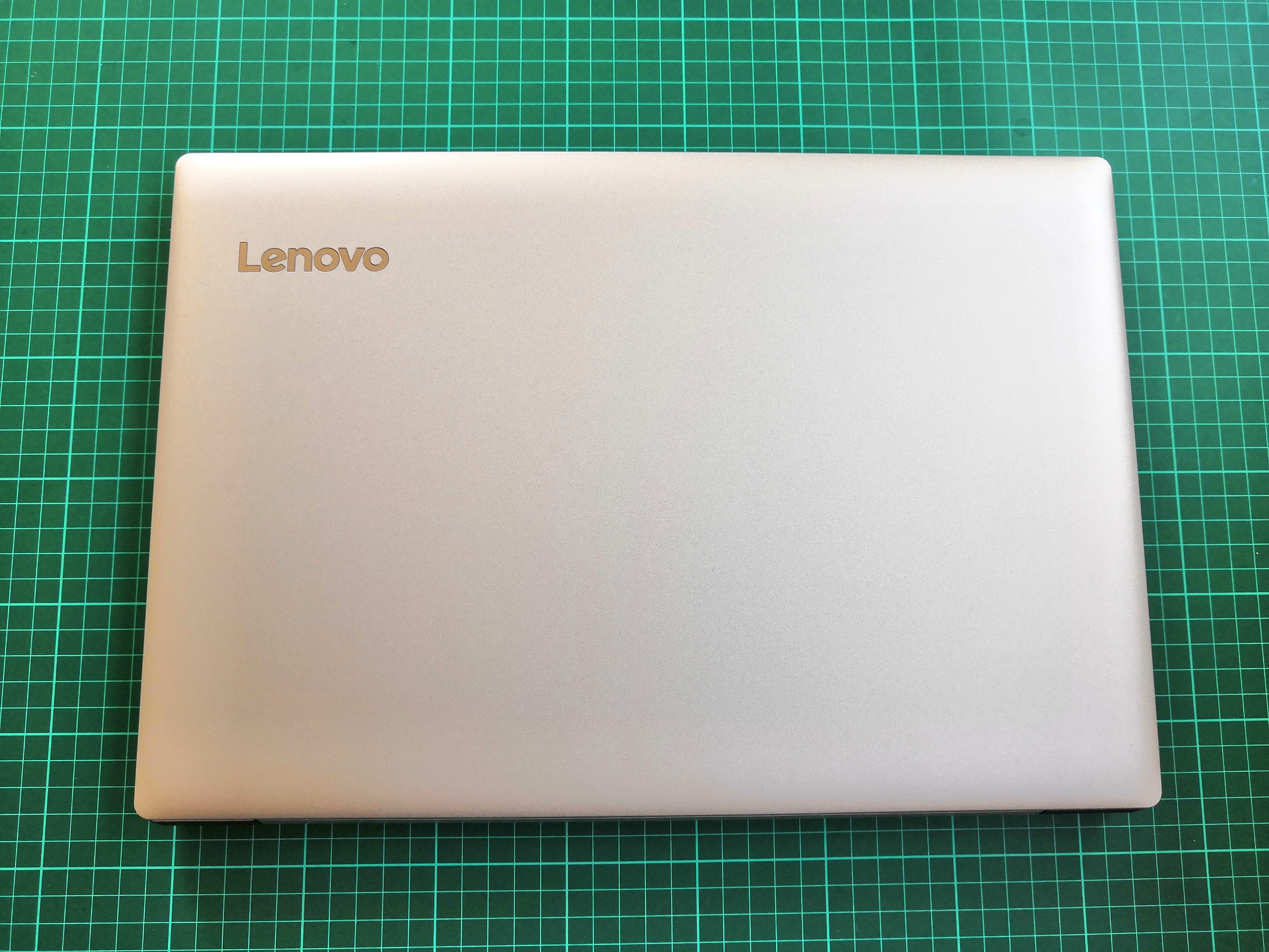
Fast forward several months later, to May 2018, and we still had not heard anything from Intel. To be ‘shipping in 2017’ but still have no product by mid-2018 was getting weirder and weirder. It wasn’t until we saw a listing for an educational laptop from a Lenovo reseller in China did we believe it actually existed.

The Lenovo IdeaPad 330-15ICN contained the i3-8121U, which is still to date the only Cannon Lake processor that has ever ‘launched’. This device is a large and bulky 15.6-inch machine with a small battery and a 13x7 inch display that was built for classrooms. Normally educational devices like this do not get put into the retail channel, however for some reason (and because it’s China), it was made available to the public.
Configurations for the device varied from a HDD and 4GB of memory, to 8GB with an SSD and HDD. It also came with discrete graphics, rather than integrated graphics, and depending on the configuration was priced from $445 to $580. I called in a few favors from friends with contacts in China, and two months later, our unit arrived. This is the unit we are reviewing here today. But that isn’t the end of the story of Intel’s 10nm product. At this point, Intel still hadn’t told us anything about the Cannon Lake processor inside.
It wasn’t until we actively posted about this laptop being available that Intel started talking about the processor. Its ARK page (Intel’s online database of processors) was now made visible to the public, and shows that the processor was officially launched in Q2 2018. Here was a dual core 15W processor with the integrated graphics disabled, and with lower clock frequencies than an almost-equivalent Kaby Lake 15W processor. Lots of questions were asked as to how the new 10nm process was, on paper, less efficient than the previous generation processor. Intel still refused to discuss exactly the changes in the hardware, or the expected performance numbers.
We since have confirmed that the graphics is indeed fused off. Intel’s official line is that this processor was released with a specific target market in mind, and it fulfils the role required. What exactly this market is, and at what price point, is still a mystery, even in 2019. However some analysts believe the graphics was a dodo out of the door due to uneconomically viable yields, as well as this chip not making any sense commercially for the product segment it ended up in – it was put into the market just to fulfil a promise to investors.
Moving from May to August, and no new processors or devices relating to Intel’s 10nm were announced. However Charlie over at SemiAccurate published knowledge that there were issues with Intel’s 10nm process as currently presented. He reports that Intel’s yields were sub-10% for the Cannon Lake 10nm CPU, well below the 60% Intel had expected at this point. He points to several issues with the process that were well behind schedule and/or expected performance: SAQP, COAG, Cobalt, and tuning – each one could be a potential showstopper if not fixed (we’ll go into these on the next page). Creating silicon is a multi-variable strategy, and turning one dial to get better characteristics in one direction might cause three other properties of the design to get worse, and finding a balance is key. What makes this process harder is when a semiconductor fab gets aggressive, and implements many changes at once, which was had been a key part of Intel’s messaging on 10nm up to this point.
Charlie’s report is that Intel was having great difficulty with the 10nm process as it was currently designed, which was a major reason for missing production targets and why the only 10nm processor up to this point is a low clocked, no-graphics version in an obscure device.
Within days of this report, but unrelated, Intel held a Data Center Summit in Santa Clara and announced that it would be bringing 10nm to the enterprise market in the form of Ice Lake Xeon Scalable (Ice Lake-SP). This would be released after Cascade Lake on 14nm (2018, actually now 2019 for general release), and Cooper Lake on 14nm (2019).

Intel was very coy to say anything about 10nm at this time. Despite repeated requests for Intel to confirm that the version of 10nm that they intend to use in Ice Lake-SP was the same as the already released Cannon Lake, representatives of the company refused to commit to any details. Part of this is because Cannon Lake is a consumer product, and Ice Lake-SP is an enterprise product, and never the twain shall meet.
No less than two weeks later, Intel made another 10nm announcement: the company would be releasing the 10nm Cannon Lake CPU in its NUC form factor. The new unit, sold under the code name Crimson Canyon, is essentially the Lenovo Ideapad laptop mentioned above but in a mini-PC form factor.

Similarly to the laptop, it uses the Core i3-8121U as the processor and due to the lack of integrated graphics it uses an RX540 AMD mobile chip for graphics. Two SO-DIMM slots are on offer, and the system comes with an M.2 slot for NVMe storage, unlike the laptop. This unit is ultimately better for thermal performance than the laptop, by virtue of being a mini-PC with a more substantial cooler. This unit, despite being announced in August 2018, didn’t actually make it on to shelves until December.
At the end of August is the annual Hot Chips conference, which is usually a hot bed for chip discussions, and Intel did not present anything new about 10nm there. It is important to remember that to date, Intel has not openly discussed Cannon Lake’s microarchitecture or improvements, for example. September was quiet, and then in October Intel held a Fall PC Event in New York.
At the Fall PC Event, Intel disclosed its 9th Gen Core processors, codenamed ‘Coffee Lake Refresh’, which included the Core i9-9900K, the Core i7-9700K, and the Core i5-9600K that came to retail a couple of weeks later. These were not 10nm, and instead we were treated to another generation of 14nm products. This is officially the fifth generation of 14nm products for the desktop, and it showed that within a process Intel has been able to make frequency and efficiency gains, as well as scale the product up to eight cores with a turbo speed of 5.0 GHz, but it was still nothing about 10nm. We were promised more news on 10nm later in the year.
Here's a table to keep up with Intel's 14nm:
| Intel's 14nm Family | |||||
| Generation | Microarchitecture | Process Node | Release Year | ||
| 1st | Broadwell | 14nm | 2014 | ||
| 2nd | Skylake | 14nm | 2015 | ||
| 3rd | Kaby Lake | 14nm+ | 2016 | ||
| 4th | Coffee Lake | 14nm++ | 2017 | ||
| 5th | Coffee Lake Refresh | 14nm++ | 2018 | ||
Very soon after the launch of the 5th Generation of 14nm, a report was released stating that Intel’s known 10nm design was, for lack of a better term, ‘dead’. The report cited core issues with some of the new parts of Intel’s design, such as COAG, which were not yielding appropriately, plus by Intel’s own admission back at Manufacturing Day, even with perfect yield, they were not expecting to meet the performance of their latest version of 14nm until the third generation of 10nm. Intel immediately refuted (via Twitter) they were ending work on 10nm, making good progress on 10nm, and improving yields consistently. Again, the company refused to state if the future of the 10nm manufacturing design was identical to that found in the 10nm processor that was already launched.
Media reports published today that Intel is ending work on the 10nm process are untrue. We are making good progress on 10nm. Yields are improving consistent with the timeline we shared during our last earnings report.
— Intel News (@intelnews) October 22, 2018
November was relatively uneventful, and in early December we finally saw the first Intel NUC devices with the Core i3-8121U for sale, starting at $530 with 8GB of DDR4 and a 1TB mechanical drive. On December 12th 2018, Intel held an Architecture Day where it started to lift the lid on its plans for 10nm, and what we should expect in 2019.
Ice Lake-U (15W) Demo Chip
This included a long discussion about its second generation 10nm product, Ice Lake, which would be coming to notebooks in a 15W form factor at the end of 2019, as well as the next two generations of cores.
| Intel Core Microarchitecture Roadmap | |||
| Core Name | Year | Process Node | Improvements |
| Broadwell | 2014 | 14nm | First Gen 14nm |
| Skylake | 2015 | 14 nm | Single Threaded Performance Lower Power Other Optimizations |
| Kaby Lake | 2016 | 14 nm+ | Frequency |
| Coffee Lake | 2017 | 14 nm++ | Frequency |
| Coffee Refresh | 2018 | 14 nm++ | Frequency |
| Sunny Cove (Ice Lake) |
2019 | 10 nm | Single Threaded Performance New Instructions Improved Scalability |
| Willow Cove | 2020 ? | 10 nm ? | Cache Redesign New Transistor Optimization Security Features |
| Golden Cove | 2021 ? | 7 / 10 nm ? | Single Threaded Performance AI Performance Networking / 5G Performance Security Features |
It is worth noting that the first generation Cannon Lake processor has ‘Cannon Lake’ cores inside, however the second generation ‘Ice Lake’ will have ‘Sunny Cove’ cores inside, which are a more radical departure in microarchitecture than the nth generation Skylake cores that Cannon Lake was based on. Details about Sunny Cove were limited, barring a mention that certain aspects of the core design had been increased.
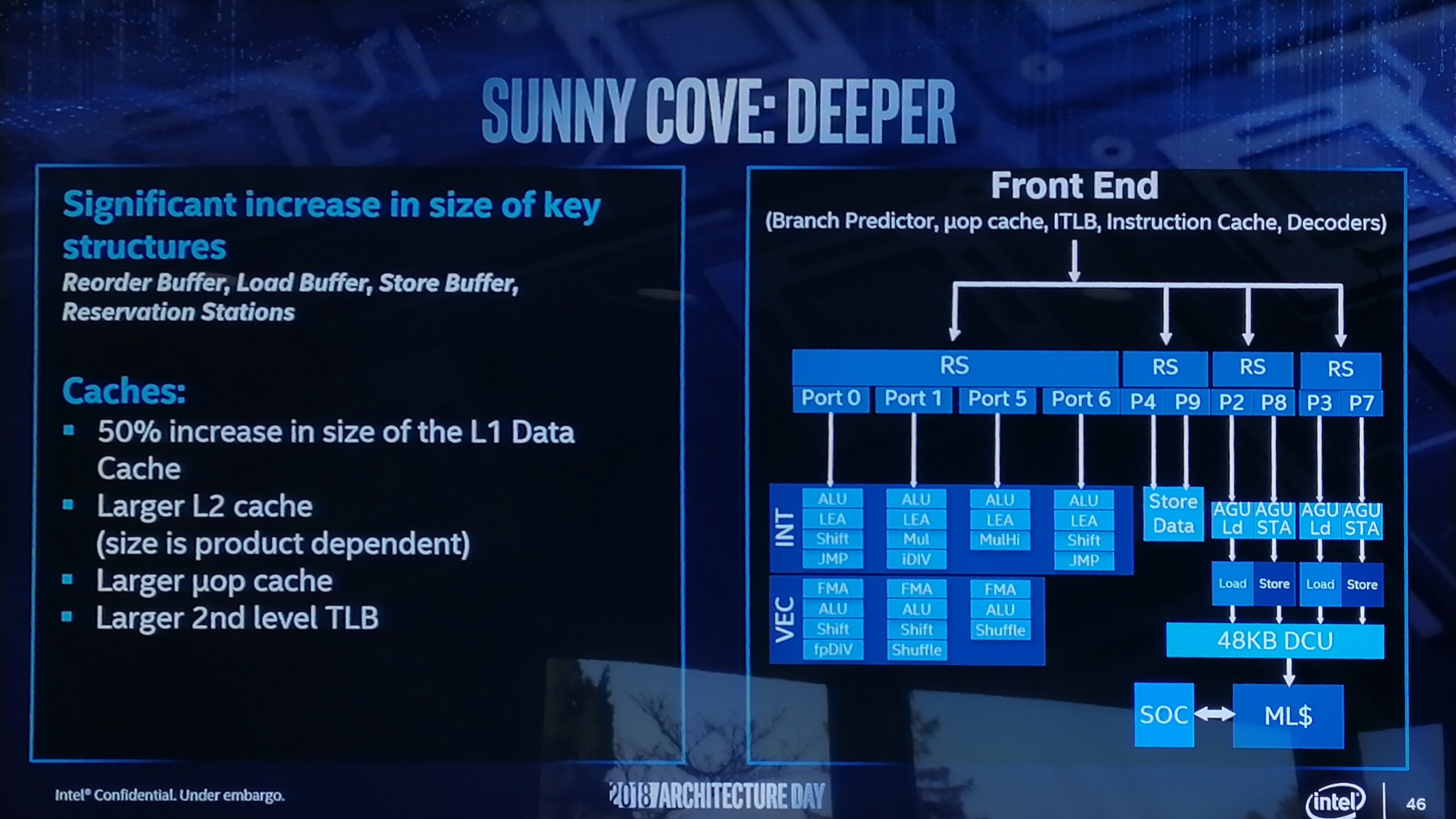
Along with Sunny Cove, Intel mentioned in a bit of detail its Gen11 graphics architecture, also set to debut on 10nm. One Intel representative stated that this was Intel's first graphics architecture on 10nm, which essentially confirms that the Cannon Lake graphics design did not work.
Also on 10nm, Intel gave its first presentation and demonstration of a new packaging technology called Foveros. This technology allows Intel to stack silicon dies on one another, and drive TSVs (through silicon vias) to connect the chips to the power plane. The demonstration chip, now known as Lakefield, used CPU and GPU cores on the top chip, with IO on the bottom chip. The idea here is that it can save x-y dimensions for products that need it. Using this technology, Intel showed its first hybrid x86 solution, with one Sunny Cove core and four Atom cores, all on 10nm. This chip is expected to be in production in late 2019.
As part of this presentation, Intel opened up a little into its manufacturing naming scheme. According to the charts, Intel is working on several versions of 10nm, known as P1274, P1273, P1222, P1274.7, and P1274.12.
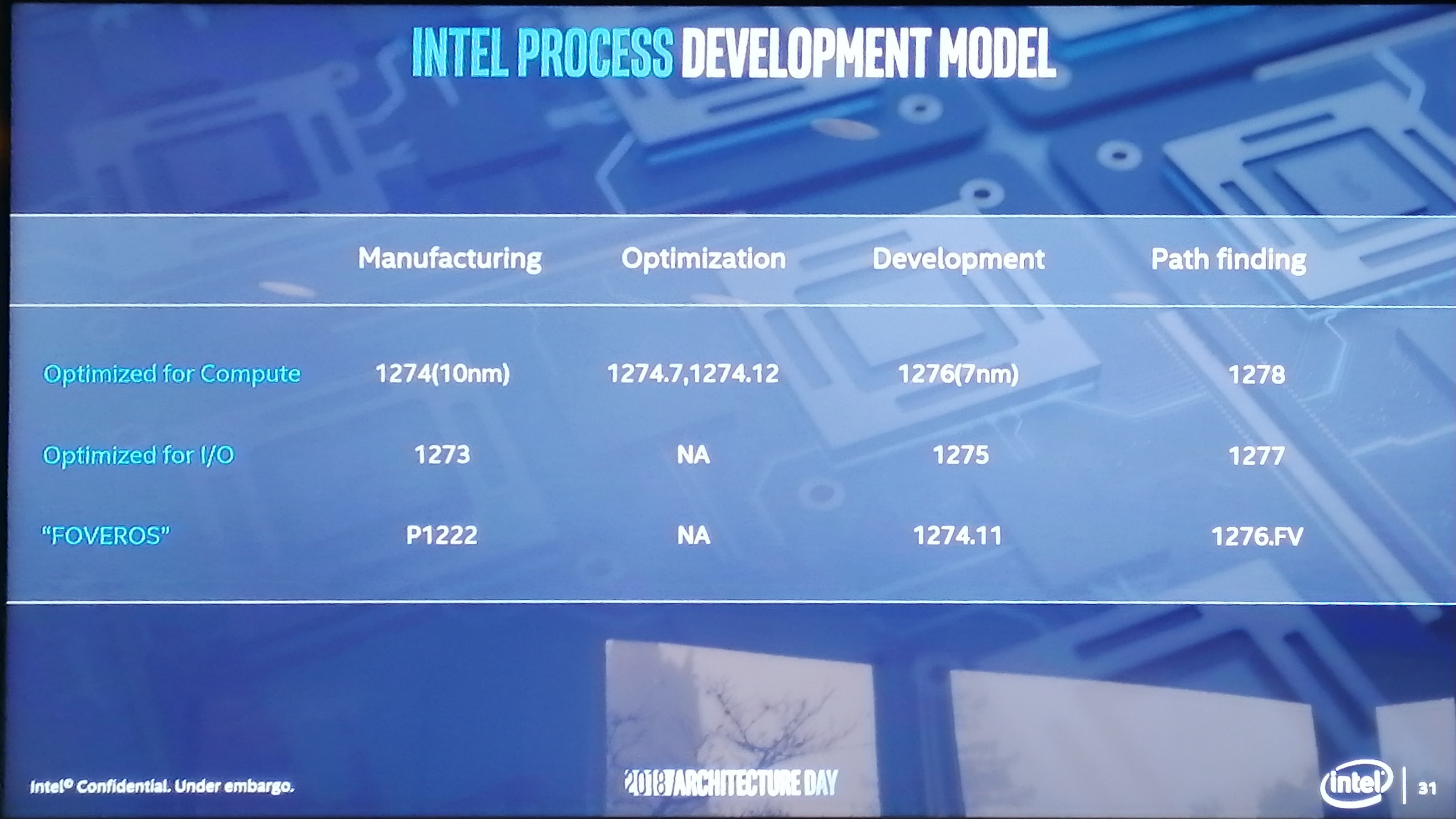
For those keeping track, these are the process names for the 10nm product lines for Ice Lake and Foveros (manufacturing), future version of 10nm (P1274.7, P1274.11), Future process nodes on 7nm (P1276, P1275), and beyond 7nm. According to Wikichip, the official process name used for Cannon Lake was P1274, suggesting that Ice Lake and Cannon Lake share the same process. However, at this time, it would appear that Intel is dropping the ‘+’ nomenclature from its 10nm and beyond products – they all fall under ‘10nm’ class, so it is impossible to say if Cannon Lake and Ice Lake share the same design layout rules.
Also presented at the Architecture Day was a server based 10nm chip - Ice Lake Xeon Scalable. According to reports, these had only entered the Intel labs a couple of weeks prior, so were quite raw in tuning. This is the chip Intel has promised for 2020 for enterprise.

As was perhaps to be expected, Intel refused to comment on the core count of this chip, the expected power consumption, and such. Typically one of Intel’s enterprise chips, even the low core count models, are in the 250mm2 or above range, which would be a sizeable leap from the 70.5mm2 on the dual core Cannon lake design.
Moving into 2019, and it marks a full year since Intel said that they were shipping 10nm for revenue at the end of 2017. So far in 2019, Intel reiterated the announcements from Architecture Day during its CES presentation, and it also introduced a new ‘Snow Ridge’ processor design built on 10nm aimed at 5G and AI workloads. Intel also clarified that it expects to see 10nm in notebooks by the end of 2019. We expect this means that desktop processors will be coming in 2020, along with enterprise processors.
That’s where we are today on Intel’s route to 10nm.


129 Comments
View All Comments
Gondalf - Friday, January 25, 2019 - link
For now they have nothing out in cpu departement, so i don't see any AMD bright year in front of us.I remember you we are already in 2019.
vegajf51 - Friday, January 25, 2019 - link
Icelake Desktop 3q 2020, intel will have another 14nm refresh before then.HStewart - Saturday, January 26, 2019 - link
Intel is expected to release 10nm+ with Covey Lake by Christmas seasons. This canon lake chip is just a test chip.pugster - Friday, January 25, 2019 - link
Thanks for the review. While the performance is not great, what about the power consumption compared with the 8130U?Yorgos - Friday, January 25, 2019 - link
it's not great obviously when you are stuck at 2.2GHz, while the prev gen cpu with the same capabilities(except the avx) can go up to 3.4GHz.I bet the 8130 would've been faster even if configured at 10Watt TDP.
Yorgos - Friday, January 25, 2019 - link
...and before jumping on me about that "stuck at 2.2GHz" let me report this:in certain loads the locked freq is slower than the unlocked one.
What does this mean? it most probably means that the unlocked freq makes the cpu run hot, throttle and then try to balance between temperature and consumption.
and a subnote on this. I think Intel should stop pushing the AVX instructions. It doesn't work as intended, it's not needed in most cases, especially when you have to design 256bit buses for 512bit data transfer on a low power cpu. Also it takes a lot of space on the die, it taxes the cache buses and it's useless when you disable your igpu(which is a good SIMD machine but not hUMA) and you have a dGPU up all the time just rendering your desktop.
They should try focusing on HSA/hUMA on their cpus+igpus instead of integrating wide SIMD instructions inside their cores.
0ldman79 - Saturday, January 26, 2019 - link
Thing is when AVX2 and AVX512 are used the performance increase can be rather massive.PCSX2, PS2 emulator, runs identically between my 3.9GHz Ivy Bridge Xeon (AVX) and my 2.8GHz i5 Skylake mobile (AVX2).
AVX2 makes several games playable. You can choose your plugin and the AVX plugin cannot play Gran Turismo 4 @ 2.8GHz, the AVX2 plugin can.
You may not find it useful, others do.
HStewart - Saturday, January 26, 2019 - link
It would be interesting to see the emulator re-factor to work with AVX 512 - it would like be twice the speed of AVX 2levizx - Sunday, January 27, 2019 - link
Nope, even with the simplest data set where AVX512 can perform twice the speed of AVX2 per cycle, the frequency has to drop significantly (~30% on Xeon Gold 5120 for example), so the upper limit is more like 40% gain. And that's PURE AVX512 code, you won't get that in real life. Assuming 50% AVX2 and 50% AVX512 code - that's a very generous assumption for non-datacentre usage, you'll have a 5% net gain.levizx - Sunday, January 27, 2019 - link
5%~20% net gain, depending on how the scaling works.