Intel's 10nm Cannon Lake and Core i3-8121U Deep Dive Review
by Ian Cutress on January 25, 2019 10:30 AM ESTCPU Performance: Memory and Power
Memory
With the same memory setup as the standard Skylake-style core, without any other improvements, we should expect Cannon Lake to perform exactly similar. Here’s a recap of the memory configuration:
| Memory Comparison | ||
| Skylake Desktop | Cannon Lake | |
| L1-D Cache |
32 KiB/core 8-way |
32 KiB/core 8-way |
| L1-I Cache |
32 KiB/core 8-way |
32 KiB/core 8-way |
| L2 Cache |
256 KiB/core 4-way |
256 KiB/core 4-way |
| L3 Cache |
2 MiB/core 16-way |
2 MiB/core 16-way |
| L3 Cache Type | Inclusive | Inclusive |
For this test we put our Cannon Lake and Kaby Lake processors through our Memory Latency Checker test. Both systems had turbo modes disabled, forcing them to run at 2.2 GHz for parity and a direct microarchitecture comparison.
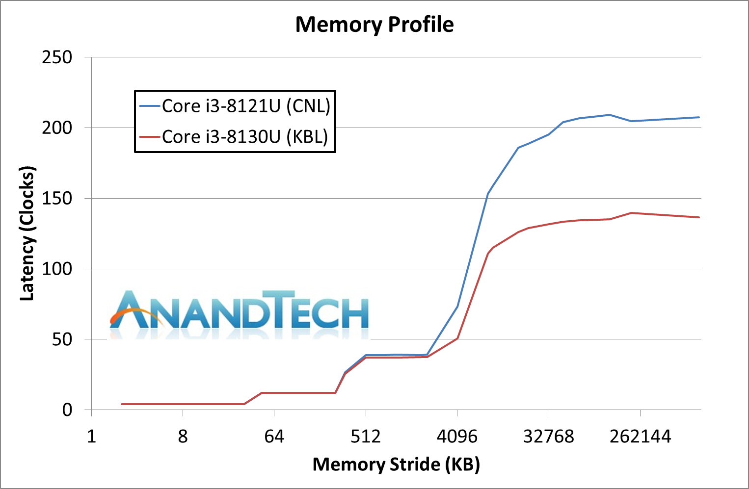
In this instance we see very little different between the two through the caches of the chip. Up to about 2MiB, both chips perform practically identical. Beyond this however, going out to main memory, there is a big discrepancy between the Kaby Lake and the Cannon Lake processor. In essence, accessing Cannon Lake main memory has an additional 50% latency.
At first we thought this was a bug. For both systems to have dual channel memory and running DDR4-2400, something had to be wrong. We double checked the setups – both systems were running in dual channel mode, giving the same memory bandwidth. The Cannon Lake processor was running at DDR4-2400 17-17-17, whereas the Kaby Lake system was at DDR4-2400 16-16-16 (due to memory SPD differences), which isn’t a big enough change to have such a big difference. The only reason we can come up with is that the memory controller on Cannon Lake must have additional overhead from the core to the memory controller – either a slower than expected PLL or something.
Power
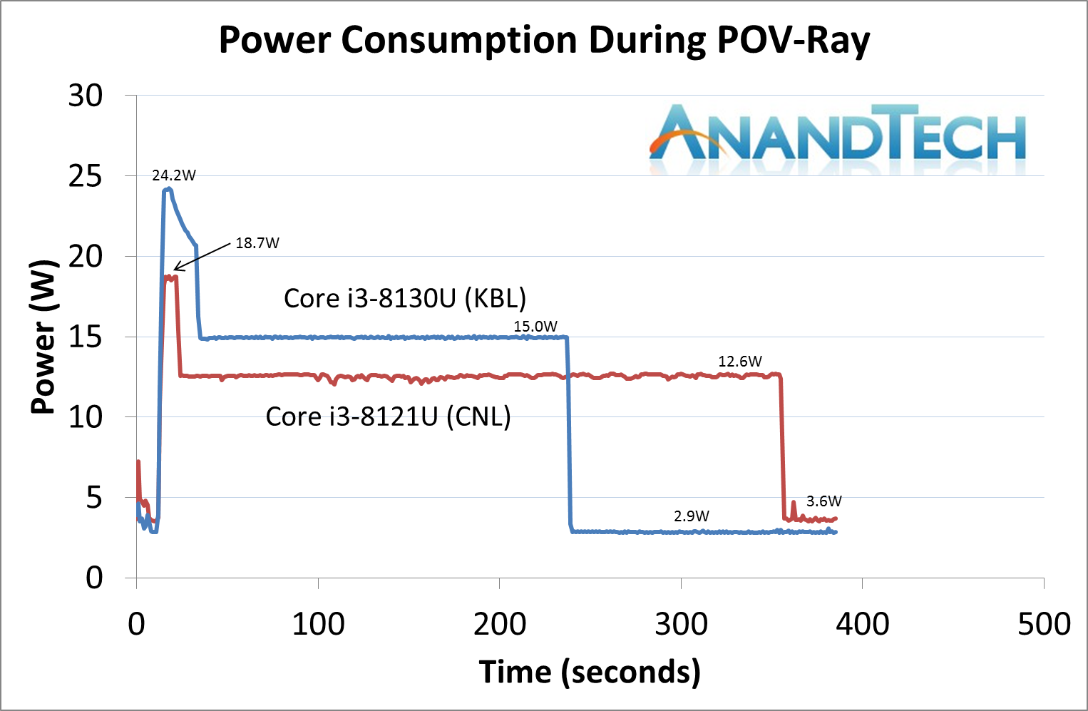
Measuring the power of these thermally limited systems is somewhat frustrating in that we are at the whims of the quality of silicon at play. Bad silicon can get hotter faster, causing thermal throttling, or it depends on how the systems are set up for the peak power numbers. We use AIDA’s power monitoring tool to give us the power numbers for the CPUs during our POV-Ray test.
If you saw our How Intel Measures TDP article, you may be familiar with the concept of Power Limits. Intel processors have several power limits set in firmware – these values are set by the system manufacturer, and Intel provides ‘guidelines’. The two key values are Power Limit 1 (PL1), which describes a steady state scenario, and Power Limit 2 (PL2) which describes a turbo scenario. The reason why the system manufacturer gets control of these is because they might put a high wattage processor into a small form factor system, and need to manage performance – this is why we sometimes see a Core i7 be outperformed by a Core i5 in the same system design.
In most cases, PL1 is set to the TDP of the processor – in this case, it should be 15W. As shown on the graph above, this is true for our Core i3-8130U system, which shows a steady state power consumption of 15.0W. The Cannon Lake processor however only peaks at 12.6W.
PL2, the turbo power of the processor, can also be determined. For the Kaby Lake processor, we see a peak of 24.2 W, while the Cannon Lake has a turbo only of 18.7 W. We see that the turbo time period for the Cannon Lake processor is also much shorter, leading to a PL1 / steady state power much sooner.
Part of this is because we are pitting the Cannon Lake laptop against the Kaby Lake mini-PC. That being said, the Cannon Lake laptop is a beefy 15.6-inch unit, and has cooling for both the CPU and the discrete RX540 graphics, which isn’t doing much during this test except showing a basic 2D display.
That is arguably a lot more cooling than the mini-PC provides, plus we are cooling it with additional fans. These settings are more a function of both Lenovo doing what it wants to in firmware that we can’t change, but also the chip as engineered.
We can also calculate some level of efficiency here. By taking the area under the graph and correcting for the base line power (2.9 W on KBL, 3.6 W on CNL), we can calculate the total power consumed during the test. We get the following:
- Core i3-8121U (CNL) consumes 867 mWh
- Core i3-8130U (KBL) consumes 768 mWh
So this means that Cannon Lake is slower in AVX2 frequency, consumes more power, and scores 25% less in POV-Ray (see previous pages). That’s damning for the design.
To further look into this data, we disabled the turbo modes on both processors and ran our POV-Ray workload adjusting the number of threads being loaded and then measured the power consumption. In this scenario we are running at the same frequency, measuring the steady state power, and are thus at the whims of both the voltage set on both processors and the efficiency. Our tool also lets us measure the power of just the cores, so we’ll plot core power against threads loaded.
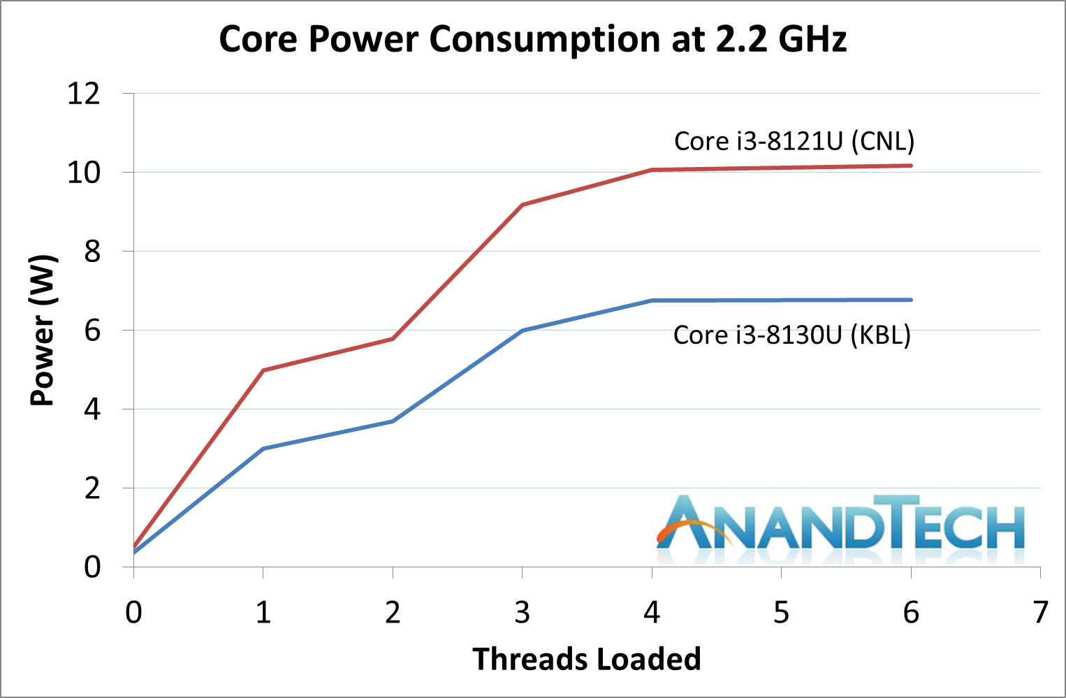
If this graph was the definitive graph, it shows that Cannon Lake is vastly inefficient (at 2.2 GHz) compared to Kaby Lake.


129 Comments
View All Comments
qcmadness - Saturday, January 26, 2019 - link
I am more curious on the manufacturing node. Zen (14 / 12nm from GF) has 12 metal layers. Cannon Lake has 13 metal layers, with 3 quad-patterning and 2 dual patterning. How would these impact the yield and manufacturing time of production? I think the 3 quad-patterning process will hurt Intel in the long run.KOneJ - Sunday, January 27, 2019 - link
More short-run I would say actually. EUV is coming to simplify and homogenize matters. This is a patch job. Unfortunately, PL analysis and comparison is not an apples-to-apples issue as there are so many facets to implementation in various design stages. A broader perspective that encompasses the overall aspects and characteristics is more relevant IMHO. It's like comparing a high-pressure FI SOHC motor with a totally unrelated low-pressure FI electrically-spooling DOHC motor of similar displacement. While arguing minutiae about design choices is interesting to satisfy academic curiosity, it's ultimately the reliability, power-curve and efficiency that people care about. Processors are much the same. As a side note, I think it's the attention to all these facets and stages that has given Jim Keller such consistent success. Intel's shaping up for a promising long-term. The only question there is where RISC designs and AMD will be when the time comes. HSA is coming, but it will be difficult due to the inherent programming challenges. Am curious to see where things are in ten or fifteen years.eastcoast_pete - Sunday, January 27, 2019 - link
Good point and question! With the GPU functions apparently simply not compatible with Intel's 10 nm process, does anyone here know if any GPUs out there that use quad-patterning at all?anonomouse - Sunday, January 27, 2019 - link
@Ian or @Andrei Is dealII missing from the spec2006fp results table for some reason? Is this just a typo/oversight, or is there some reason it's being omitted?KOneJ - Sunday, January 27, 2019 - link
Great write up, but isn't this backwards on the third page?"a 2-input NAND logic cell is much smaller than a complex scan flip-flop logic cell"
"90.78 MTr/mm^2 for NAND2 gates and 115.74 MTr/mm^2 for Scan Flip Flops"
NAND cell is smaller than flip-flop cell, but there is more flip-flop than NAND in a square millimeter?
Or am I missing something?
Rudde - Sunday, January 27, 2019 - link
A NAND logic cell consists of 2 transistors, while a Scan flip flop logic cell can consist of different count of transistors depending on where it is used. If I remeber correctly, Intel uses 8, 10 and 12 transistor designs.That gives 45.39 million NAND cells per mm² (basically SRAM) and ~12 million flip-flop cells.
The NAND cell is smaller because it consists of fewer transistors.
KOneJ - Sunday, January 27, 2019 - link
It would be great if you guys could get a CNL sample in the hands of Agner Fog. He might be able to answer some of the micro-architecture questions through his tests.dragosmp - Sunday, January 27, 2019 - link
Awesome review, great in depth content and well explained. Considering the amount of work this entailed, it's clear why these reviews don't happen every day. Thanksdragosmp - Sunday, January 27, 2019 - link
I'll just add...many folks are saying AMD should kick arse. They should, but Intel has been in this situation before - they had messed up the 90nm process; probably not quite as bad as the chips to be unusable, but it opened the door to AMD and its Athlon 64. What did AMD do? Messed it up in turn with slow development and poor design choices. Hopefully they'll capitalize this time so that we get an actual dupoloy, rather than the monopoly on performance we had since Intel's 65nm chips.eva02langley - Sunday, January 27, 2019 - link
Euh... You mean this...?https://www.youtube.com/watch?v=osSMJRyxG0k
Anti-competitive tactics? They bought the OEM support to prevent competition.
And, all lately, this came up...
https://www.tomshardware.com/news/msi-ceo-intervie...
"Relationship with Intel: Chiang told us that, given Intel's strong support during the shortage, it would be awkward to tell Intel if he chose to come out with an AMD-powered product. "It's very hard for us to tell them 'hey, we don't want to use 100 percent Intel,' because they give us very good support," he said. He did not, however, make any claims that Intel had pressured him or the company."
Yeah right, Intel is winning because they have better tech... /sarcasm