Intel's 10nm Cannon Lake and Core i3-8121U Deep Dive Review
by Ian Cutress on January 25, 2019 10:30 AM ESTConclusion: I Actually Used the Cannon Lake Laptop as a Daily System
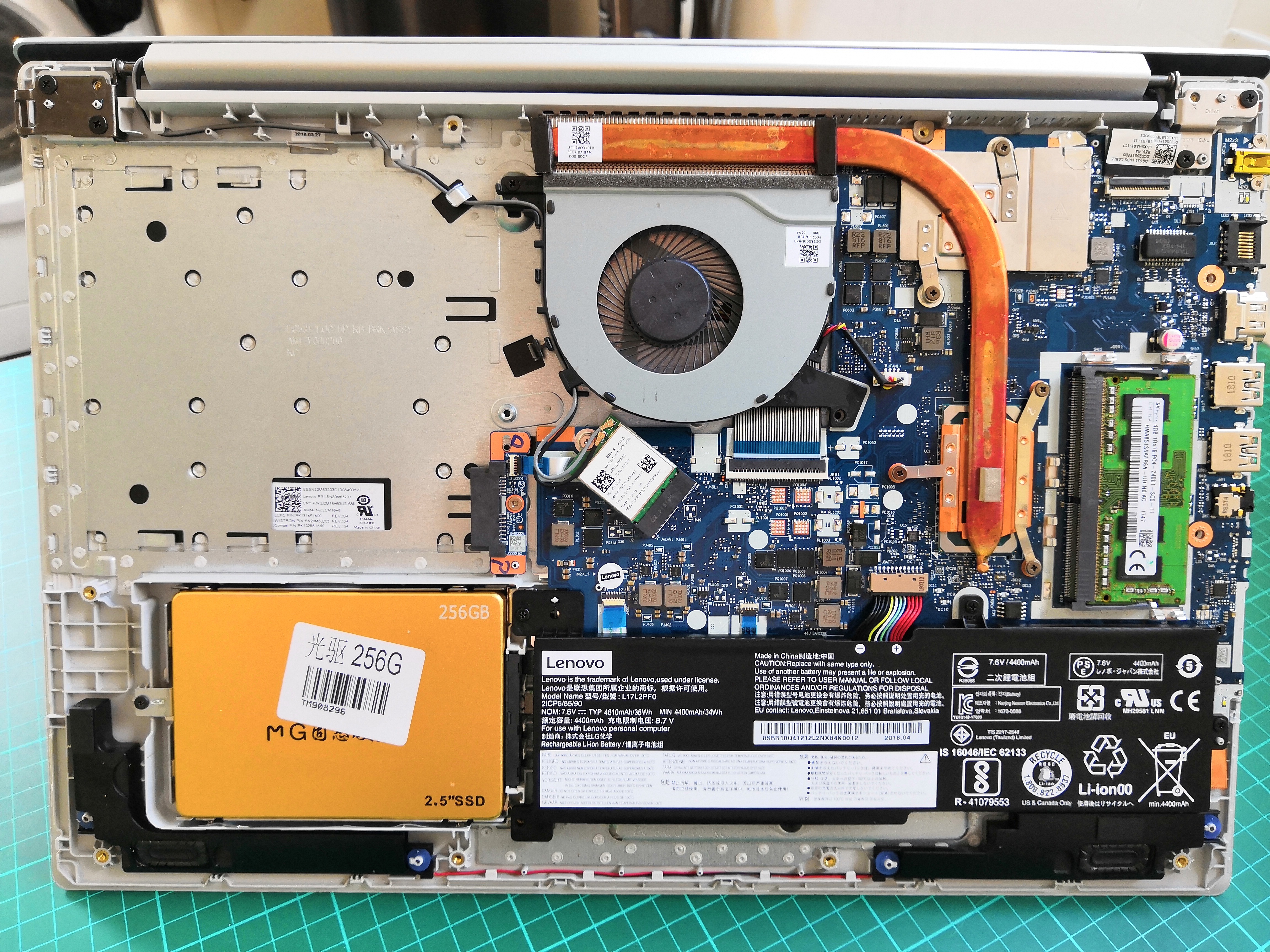
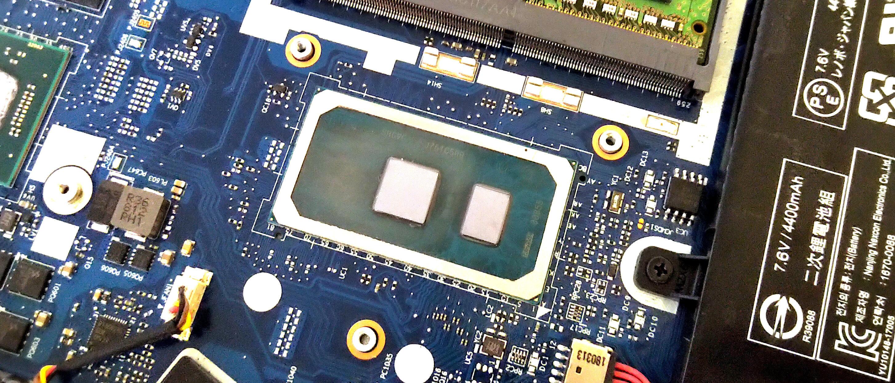
When we ordered the Lenovo laptop, not only was I destined to test it to see how well Intel’s 10nm platform performs, but I also wanted to see what the device was like to actually use. Once I’d removed the terrible drives it came with and put in a 1TB Crucial MX200 SSD, I started to put it to good use.
The problem with this story is that because this is a really bad configuration of laptop, it gives the hardware very little chance to show its best side. We covered this in our overview of Carrizo several years ago, after OEM partners kept putting chips with reasonable performance into the worst penny pinching designs. The same thing goes with this laptop – it is an education focused 15.6-inch laptop whose screen is only 1366x768, and the TN panel’s best angle to view is as it is tilted away from you. It is bulky and heavy but only has a 34 Wh battery, whereas the ideal laptop is thin and light and lasts all day on a single charge. From the outset, using this device was destined to be a struggle.
I first used the device when I attended Intel’s Data Summit in mid-August. On the plane I didn’t have any space issues because I had reserved a bulkhead economy seat, however after only 4 hours or so of light word processing on a low screen brightness, I was already out of battery. Thankfully I could work on other things on my second laptop (always take two laptops to events, maybe not day-to-day at a show, but always fly with two). At the event, I planned to live blog the day of presentations. This means being connected online, uploading text, and being of a sufficient brightness to see the screen. After 90 minutes, I had 24% battery left. This device has terrible battery life, a terrible screen, is bulky, and weighs a lot.
I will say this though, it does have several positives. Perhaps this is because the RX540 is in the system, but the Windows UI was very responsive. Now of course this is a subjective measure, however I have used laptops with Core i7 and MX150 hardware that were slower to respond than this. It did get bogged down when I went into my full workflow with many programs, many tabs, and many messaging software tools, but I find that any system with only 8GB of memory will hit my workflow limits very quickly. On the natural responsiveness front, I can’t fault it.
Ultimately I haven’t continued to use the laptop much more – the screen angle required to get a good image, the battery life, and the weight are all critical issues that individually would cause me to ditch the unit. At this price, there are plenty of Celeron or Atom notebooks that would fit the bill and feel nicer to use. I couldn’t use this Ideapad unit with any confidence that I would make it through an event, either a live blog or a note taking session, without it dying. As a journalist, we can never guarantee there will be a power outlet (or an available power outlet) at the events we go to, so I always had to carry a second laptop in my bag regardless. The issue is that the second laptop I use often lasts all day at an event on its own.
Taking Stock of Intel’s 10nm Cannon Lake Design
When we lived in a world with Intel’s Tick Tock, Cannon Lake would be a natural tick – a known microarchitecture with minor tweaks but on a new process node. The microarchitecture is a tried and tested design, as we now have had four generations of it from Skylake to Coffee Lake Refresh, however the chip just isn’t suitable for prime time.
Looking at how Intel has presented its improvements on 10nm, with features like using Cobalt, Dummy Gates, Contact Over Active Gates, and new power design rules, if we assume that every advancement works perfectly then 10nm should have been a hit out of the gate. The problem is, semiconductor design is like having 300 different dials to play with, and tuning one of those dials causes three to ten others to get worse. This is the problem Intel has had with 10nm, and it is clear that some potential features work and others do not – but the company is not saying which ones for competitive and obvious reasons.
At Intel’s Architecture Day in December, the Chief Engineering Officer Dr. Murthy Renduchintala was asked if the 10nm design had changed. His response was contradictory and cryptic: ‘It is changing, but it hasn’t changed’. At that event the company was firmly in the driving seat of committing to 10nm by the end of 2019, in a quad core Ice Lake mobile processor, in a new 3D packaging design called Lakefield, in an Ice Lake server CPU for 2020, and in a 5G/AI focused processor called Snow Ridge. Whatever 10nm variant of the process they’re planning to use, we will have to wait and see.
I’ll go back to this slide that Intel presented back at the Technology and Manufacturing Day:
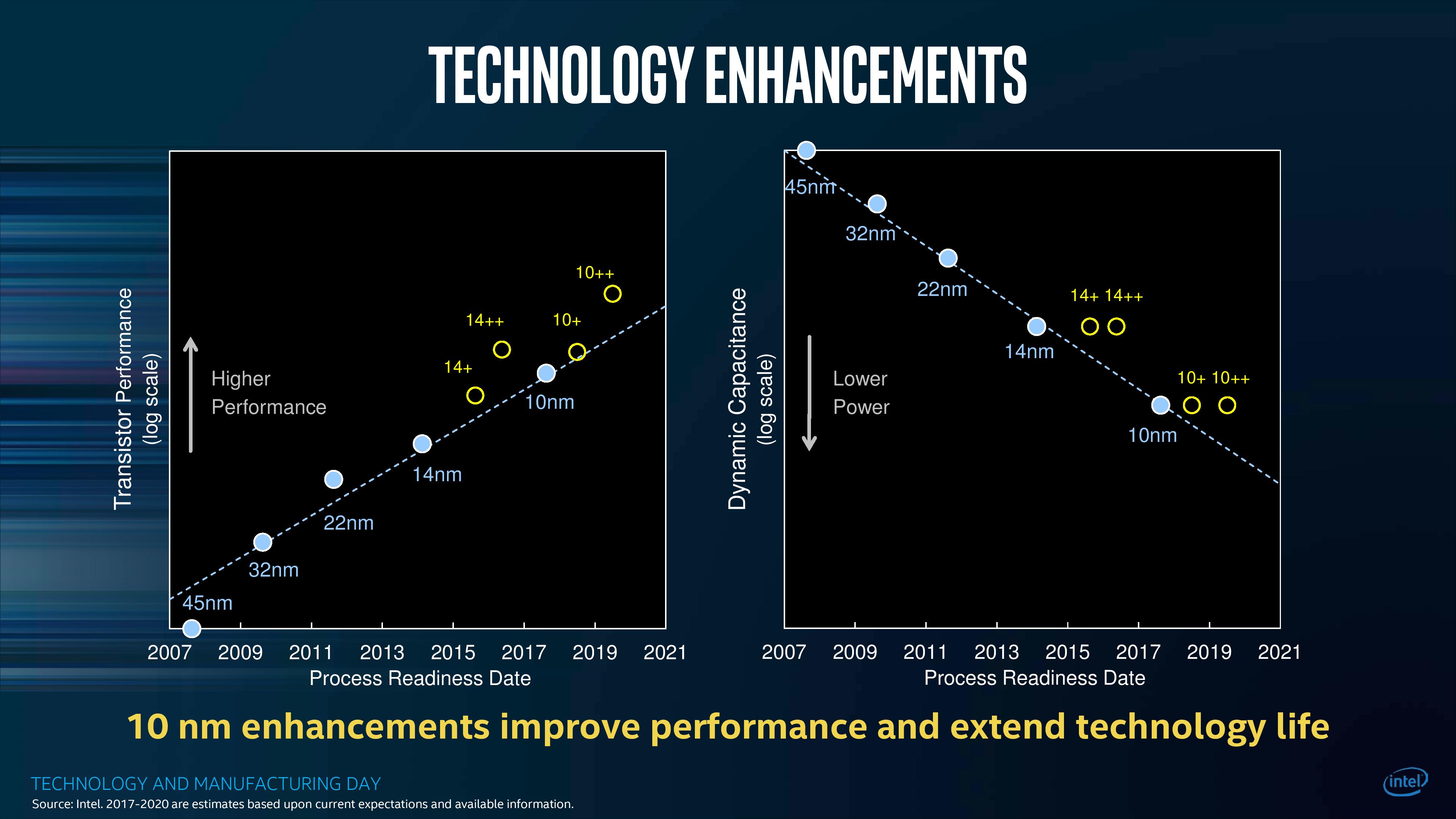
In this slide it shows on the right that 10nm (and its variants) have lower power through lower dynamic capacitance. However, on the left, Intel shows both 10nm (Cannon Lake) and 10nm+ (Ice Lake) as having lower transistor performance than 14nm++, the current generation of Coffee Lake processors.
This means we might not see a truly high-performance processor on 10nm until the third generation of the process is put into place. Right now, based on our numbers on Cannon Lake, it’s clear that the first generation of 10nm was not ready for prime time.
Cannon Lake: The Blip That Almost Didn’t Happen
We managed to snap up a Cannon Lake chip by calling in a few favors to buy it from a Chinese reseller who I’m pretty sure should not have been selling them to the public. They were educational laptops that may not have sold well, and the reseller just needed to get rid of them. Given Intel’s reluctance to talk about anything 10nm at CES 2018, and we find that the chips ‘shipped for revenue’ end up in a backwater design like this, then it would look like that Intel was trying to hide them. That was our thought for a good while, until Intel announced the Cannon Lake NUC. Even then, from launch announcement to being at general retail took four months, and by that time most people had lost interest.
At some point Intel had to make good on its promises to investors by shipping something 10nm to somewhere. Exactly how many chips were sold (and to whom) is not discussed by Intel, but I have heard some numbers flying around. Based on our performance numbers, it’s obvious why Intel didn’t want to promote it. On the other hand, at least being told about it beyond a simple sentence would have been nice.
After testing the chip, the only way I’d recommend one of these things is for the AVX512 performance. It blows everything else in that market out of the water, however AVX512 enabled programs are few and far between. Plus, given what Intel has said about the Sunny Cove core, that part will have it instead. If you really need AVX512 in a small form factor, Intel will sell you a NUC.
Cannon Lake, and the system we have with it inside, is ultimately now nothing more than a curio on the timeline of processor development. Which is where it belongs.


129 Comments
View All Comments
qcmadness - Saturday, January 26, 2019 - link
I am more curious on the manufacturing node. Zen (14 / 12nm from GF) has 12 metal layers. Cannon Lake has 13 metal layers, with 3 quad-patterning and 2 dual patterning. How would these impact the yield and manufacturing time of production? I think the 3 quad-patterning process will hurt Intel in the long run.KOneJ - Sunday, January 27, 2019 - link
More short-run I would say actually. EUV is coming to simplify and homogenize matters. This is a patch job. Unfortunately, PL analysis and comparison is not an apples-to-apples issue as there are so many facets to implementation in various design stages. A broader perspective that encompasses the overall aspects and characteristics is more relevant IMHO. It's like comparing a high-pressure FI SOHC motor with a totally unrelated low-pressure FI electrically-spooling DOHC motor of similar displacement. While arguing minutiae about design choices is interesting to satisfy academic curiosity, it's ultimately the reliability, power-curve and efficiency that people care about. Processors are much the same. As a side note, I think it's the attention to all these facets and stages that has given Jim Keller such consistent success. Intel's shaping up for a promising long-term. The only question there is where RISC designs and AMD will be when the time comes. HSA is coming, but it will be difficult due to the inherent programming challenges. Am curious to see where things are in ten or fifteen years.eastcoast_pete - Sunday, January 27, 2019 - link
Good point and question! With the GPU functions apparently simply not compatible with Intel's 10 nm process, does anyone here know if any GPUs out there that use quad-patterning at all?anonomouse - Sunday, January 27, 2019 - link
@Ian or @Andrei Is dealII missing from the spec2006fp results table for some reason? Is this just a typo/oversight, or is there some reason it's being omitted?KOneJ - Sunday, January 27, 2019 - link
Great write up, but isn't this backwards on the third page?"a 2-input NAND logic cell is much smaller than a complex scan flip-flop logic cell"
"90.78 MTr/mm^2 for NAND2 gates and 115.74 MTr/mm^2 for Scan Flip Flops"
NAND cell is smaller than flip-flop cell, but there is more flip-flop than NAND in a square millimeter?
Or am I missing something?
Rudde - Sunday, January 27, 2019 - link
A NAND logic cell consists of 2 transistors, while a Scan flip flop logic cell can consist of different count of transistors depending on where it is used. If I remeber correctly, Intel uses 8, 10 and 12 transistor designs.That gives 45.39 million NAND cells per mm² (basically SRAM) and ~12 million flip-flop cells.
The NAND cell is smaller because it consists of fewer transistors.
KOneJ - Sunday, January 27, 2019 - link
It would be great if you guys could get a CNL sample in the hands of Agner Fog. He might be able to answer some of the micro-architecture questions through his tests.dragosmp - Sunday, January 27, 2019 - link
Awesome review, great in depth content and well explained. Considering the amount of work this entailed, it's clear why these reviews don't happen every day. Thanksdragosmp - Sunday, January 27, 2019 - link
I'll just add...many folks are saying AMD should kick arse. They should, but Intel has been in this situation before - they had messed up the 90nm process; probably not quite as bad as the chips to be unusable, but it opened the door to AMD and its Athlon 64. What did AMD do? Messed it up in turn with slow development and poor design choices. Hopefully they'll capitalize this time so that we get an actual dupoloy, rather than the monopoly on performance we had since Intel's 65nm chips.eva02langley - Sunday, January 27, 2019 - link
Euh... You mean this...?https://www.youtube.com/watch?v=osSMJRyxG0k
Anti-competitive tactics? They bought the OEM support to prevent competition.
And, all lately, this came up...
https://www.tomshardware.com/news/msi-ceo-intervie...
"Relationship with Intel: Chiang told us that, given Intel's strong support during the shortage, it would be awkward to tell Intel if he chose to come out with an AMD-powered product. "It's very hard for us to tell them 'hey, we don't want to use 100 percent Intel,' because they give us very good support," he said. He did not, however, make any claims that Intel had pressured him or the company."
Yeah right, Intel is winning because they have better tech... /sarcasm