TechInsights Publishes Apple A12 Die Shot: Our Take
by Andrei Frumusanu on September 25, 2018 11:50 AM EST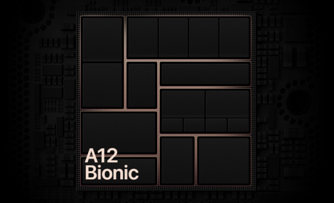
As is custom by now every year, we look forward to TechInsights teardown of the latest new mobile SoCs. This time around we’re delighted to see a new die shot of the new Apple A12, the first commercially available 7nm piece of silicon.
While TechInsights posted their take on the block identification and labelling, found on their iPhone XS teardown blog post, I do think it missed the mark in terms of the CPU complexes. Therefore I did my own analysis and took the liberty of adding a bit more visibility and custom labelling of the die shot:

AnandTech modified TechInsights Apple A12 Die Shot
We see two big cores in the centre-left next to what TechInsights labelled as the NPU. The cores have seen some larger restructuring and this is most obvious in the doubling of the SRAM macros of the L1 data caches which I’ve confirmed to be tested at 128KB – twice the size over last year’s 64KB of the A11 cores. We also similarly see a doubling of the L1 instruction cache macro cells – which also likely hints that this has also seen a doubling to up to 128KB.
The CPU complex cache remains largely the same size as on the A11, with the only difference being a re-layout in a more clean manner. I have big expectations of this part of the new microarchitecture, something we’ll dwell more deeply in our upcoming full review.
The small cores are found in the bottom centre – four of them surrounding their L2 cache logic and memory banks.
The system cache block of the A12 has seen a very major redesign, as opposed to the A11 and prior SoCs, we see a very obvious slice separation into four units. Ironically, at least on the die, this looks a lot more to what we’ve seen in the Snapdragon 845 system cache block.
On the GPU side of things, it’s very clear that this is very much a direct successor to last year’s GPU as the blocks structure in the common shared logic and inside a GPU core is pretty much in line with what we’ve seen last year. We’ll be dwelling into GPU IP discussions more in our upcoming review.
We break down the individual IP block sizes alongside the total die size in the following table:
| Die Block Comparison (mm²) | ||
| SoC Process Node |
Apple A12 TSMC N7 |
Apple A11 TSMC 10FF |
| Total Die | 83.27 | 87.66 |
| Big Core | 2.07 | 2.68 |
| Small Core | 0.43 | 0.53 |
| CPU Complex (incl. cores) | 11.90 | 14.48 |
| GPU | 14.88 | 15.28 |
| GPU Core | 3.23 | 4.43 |
In terms of determining the actual process node shrink, the closest valid apples-to-apples comparison we can make are in the small cores and an individual GPU core. Here we see a shrink from 0.53mm² to 0.43mm² in the small CPU cores – representing a 23% reduction. On the GPU core side we see a more significant 37% reduction down from 4.43mm² to 3.23mm².
All in all Apple is again at the leading edge of manufacturing technology and the new A12 showcases some really interesting changes in its silicon blocks. Stay tuned for our full iPhone XS and XS Max review in the near term future.
Source: TechInsights


34 Comments
View All Comments
Andrei Frumusanu - Tuesday, September 25, 2018 - link
It's a SoC wide cache level.name99 - Tuesday, September 25, 2018 - link
Each of those separate blocks has a 64-bit controller CPU called Chinook. Chinook is a type of (non-vortex) wind, which suggests that it's from the Zephyr/Mistral/Tempest family. Examinations of the code that these run (firmware BLOBs in iOS12 that are presumably things like initialization and power management --- and at least some aspects of scheduling for the GPU) reveal FP instructions but no NEON, so they may be something like a Tempest or Zephyr with NEON stripped down to minimal FP.There's also an FPGA on the SoC. This Lattice FPGA has been there since the A7 and we still don't know how it's used. And there's also the M12 (motion coprocessor) which I expect has some tiny ARM core on it. (Maybe Apple now designs those, or maybe it's still vanilla ARM.)
skavi - Thursday, September 27, 2018 - link
Hey, you seem knowledgeable about this stuff. I have a really dumb question that I've never known where to ask: what's in the unlabeled area of SoCs? I know with Android there's typically a modem there, but what fills the rest of the space? Thanks!name99 - Thursday, September 27, 2018 - link
There's LOTS of stuff, some known, some not. Includes- Secure enclave (separate core, separate storage)
- ISP (camera processing)
- media encoder/decoder (video and audio)
- M12 (motion coprocessor, detects acceleration and rotation, provides orientation info for AR, supports raise to wake and [I think] "Hey Siri" functionality, ie always listening for that phrase even when screen is dark
- flash controller (and a few other small IO controllers).
+ The big IO (cell, wifi, BT, GPS) is still off chip. Apple has enough know-how now to create W3 (WiFi and BT) but W3 WiFi is still way behind state of the art (no MIMO, just 2.4GHz, very much bare minimum to solve certain tasks and no more).
- There's also known to be a Lattice FPGA on the SoC (one has been there since the A7), but as far as I know we STILL don't know how it's used...
qzy__ - Tuesday, September 25, 2018 - link
It seems that A11 has 3MB private L2 each Monsoon core. Also, it has 2MB L2 which 4 Mistral small cores shared with, but it is likely that the two big cores can access all 8M L2 simultaneously. I'm looking forward you can analyse how the L2 cache one the A12 chip works.Tigran - Tuesday, September 25, 2018 - link
Andrei, could you please make clear - is GPU (14.88) also incl. cores, like CPU? And what about NPU - no figures?ikjadoon - Tuesday, September 25, 2018 - link
>Therefor I did my own analysis and took the liberty of adding a bit more visibility and custom labelling of the die shotI think "therefore" is the one wanted, not "therefor". "Therefor" means "for it", but "therefore" is a conjunction meaning "as a result".
https://www.grammarly.com/blog/therefore-vs-theref...
porcupineLTD - Tuesday, September 25, 2018 - link
Thank you for the insightful contribution, this site would be nothing without comments like yours!pukemon1976 - Tuesday, September 25, 2018 - link
why don't you apply to anandtech?damianrobertjones - Wednesday, September 26, 2018 - link
Cool. It's great to learn. Thank you!