The iPhone XS & XS Max Review: Unveiling the Silicon Secrets
by Andrei Frumusanu on October 5, 2018 8:00 AM EST- Posted in
- Mobile
- Apple
- Smartphones
- iPhone XS
- iPhone XS Max
The A12 Tempest CPU µarch: A Fierce Small Core
Apple had first introduced a “small” CPU core alongside the Twister cores in the A10 SoC, powering the iPhone 7 generation. We’ve never really had the opportunity to dissect these cores, and over the years there was a bit of mystery around them as to what they’re capable of.
Apple’s introduction of a heterogeneous CPU topology in one sense was one of the biggest validations for Arm designs. Having separate low(er)-power CPUs on a SoC is a simple matter of physics: It’s just not possible to have bigger microarchitectures scale down power as efficiently as if you would just use a separate smaller block. Even in a mythical perfectly clock-gated microarchitecture, you would not be able to combat the static leakage present in bigger CPU cores, and thus this would come with the negative consequence of being part of the everyday power consumption on a device, even for small workloads. Power gating the big CPU cores, and instead shifting to much smaller CPU in contrast, helps alleviate static leakage, as well as (if designed as such) improving the dynamic leakage power efficiency.
The Tempest cores in the A12 are now the third iteration of this “small” microarchitecture, and since the A11 they are now fully heterogeneous and work independently of the big cores. But the question is, is this actually the third iteration, or did Apple do something more interesting?
The Tempest core is a 3-wide out-of-order microarchitecture: Already out of the gate this means it has very little to do with Arm’s own “little” cores, such as the A53 and A55, as these are simpler in-order designs.
The Tempest core’s execution pipelines are also relatively few: There are just two main pipelines that are capable of simple ALU operations; meanwhile one of them also does integer and FP multiplications, and the other is able to do FP additions. Essentially we just have two primary execution ports to each of the more complex pipelines behind them. Meanwhile in addition to the two main pipelines, there’s also a dedicated combined load/store port.
Now what is very interesting here is that this essentially looks identical to Apple’s Swift microarchitecture from Apple's A6 SoC. It’s not very hard to imagine that Apple would have recycled this design, ported it to 64-bit, and they now use it as a lean out-of-order machine serving as the lower power CPU core. If this is indeed Swift derived, then on top of the three execution ports described above, we should also find a dedicated port for integer and fp divisions, such as not to block the main pipelines whenever such an instruction is fed.
The Tempest cores clock up to a maximum of 1587MHz and are served by 32KB instruction and data caches, as well as an increased shared 2MB L2 cache that uses power management to partially power down SRAM banks.
In terms of power efficiency, the Tempest cores were essentially my prime candidate to try to get to some sort of apples-to-apples comparison between the A11 and A12 for power efficiency. I haven’t seen major differences in the cores besides the bigger L2, and Apple has also kept the frequencies similar. Unfortunately, "similar" isn't identical in this case; because the small cores on the A11 can boost up to 1694MHz when there’s only one thread active on them, I had no really good way to also measure performance at iso-frequency.
I did run SPEC at an equal 1587MHz frequency by simply having a second dummy thread spinning on another core while the main workloads were benchmarking. And I did try to get some power figures through this method by regression testing the impact of the dummy thread. However the power was near identical to the figures I measured at 1694MHz. As a result I dropped the idea, and we'll just have to just keep in mind that the A11’s Mistal cores were running 6.7% faster in the following benchmarks:
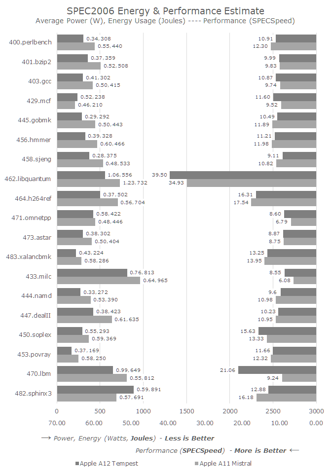
Much like on the Vortex big cores, the biggest improvements for the new Tempest cores are found in the memory-sensitive benchmarks. The benchmarks in which Tempest loses to Mistral are mainly execution bound, and because of the frequency disadvantage, there’s no surprise that the A12 lost in this particular single-threaded small core scenario.
Overall, besides the memory improvements, the new Tempest cores looks very similar in performance to last year’s Mistral cores. This is great as we can also investigate the power efficiency, and maybe learn something more concrete about the advantages of TSMC's 7nm manufacturing process.
Unfortunately, the energy efficiency improvements are somewhat inconclusive, and more so maybe disappointing. Looking at the SPECint2006 workloads overall, the Tempest-powered A12 was 35% more energy efficient than the Mistral-powered A11. Because the Mistral cores were running at a higher frequency in this test, the actual efficiency gains for A12 would likely be even less at an ISO-frequency level. Granted, we’re still looking at a general ISO-performance comparison here, as the memory improvements in A12 were able to push the Tempest cores to an integer suite score nearly identical to the higher-clocked Mistral cores.
In the overall FP benchmarks, Tempest was only 17% more efficient, even though it did perform better than the A11’s Mistral cores.
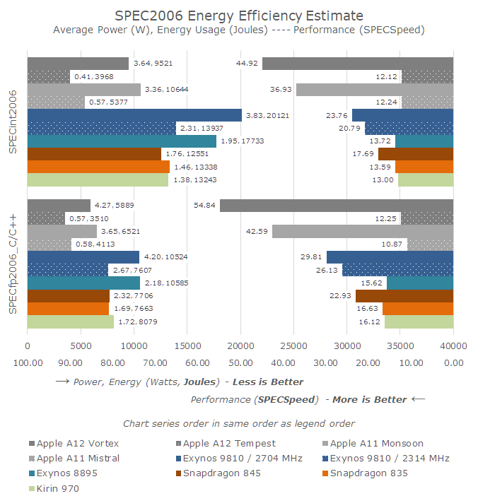
Putting the A11 and A12 small cores in comparison with their big brothers as well as the competition from Arm, there’s not much surprise in terms of the results. Compared to the big Apple cores, the small cores only offer a third to a fourth of the performance, but they also use less than half the energy.
What did surprise me a lot was seeing just how well Apple’s small cores compare to Arm’s Cortex-A73 under SPECint. Here Apple’s small cores almost match the performance of Arm’s high-performance cores from ust 2 years ago. In SPEC's integer workloads, A12 Tempest is nearly equivalent to a 2.1GHz A73.
However in the SPECfp workloads, the small cores aren’t competitive. Not having dedicated floating-point execution resources puts the cores at a disadvantage, though they still offer great energy efficiency.
Apple’s small cores in general are a lot more performant that one would think. I’ve gathered some incomplete SPEC numbers on Arm’s A55 (it takes ages!) and in general the performance difference here is 2-3x depending on the benchmark. In recent years I’ve felt that Arm’s little core performance range has become insufficient in many workloads, and this may also be why we’re going to see a lot more three-tiered SoCs (such as the Kirin 980) in the coming future. As it stands, the gap between the maximum performance of the little cores and the most efficient low performance point of the big continues to grow into one direction. All of which makes me wonder whether it’s still worth it to stay with an in-order microarchitecture for Arm's efficiency cores.
Neural Network Inferencing Performance on the A12
Another big, mysterious aspect of the new A12 was the SoC's new neural engine, which Apple advertises as designed in-house. As you may have noticed in the die shot, it’s a quite big silicon block, very much equaling the two big Vortex CPU cores in size.
To my surprise, I found out that Master Lu’s AImark benchmark also supports iOS, and better still it uses Apple's CoreML framework to accelerate the same inference models as on Android. I ran the benchmark on the latest iPhone generations, as well as a few key Android devices.
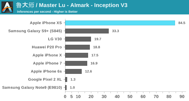
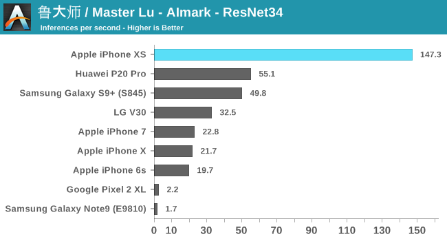
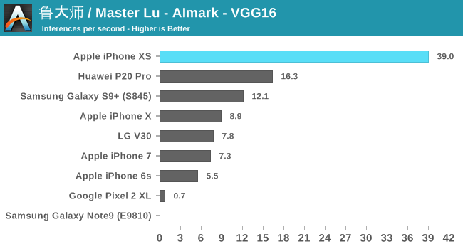
Overall, Apple’s 8x performance claims weren’t quite confirmed in this particular test suite, but we see solid improvements of 4-6.5x. There’s one catch here in regards to the older iPhones: as you can see in the results, the A11-based iPhone X performs quite similarly to previous generation phones. What’s happening here is that Apple’s executing CoreML on the GPU. It seems to me that the NPU in the A11 might have never been exposed publicly via APIs.
The Huawei P20 Pro’s Kirin 970 falls roughly 2.5x behind the new A12 – which coincidentally exactly matches the advertised 2TOPs vs 5TOPs throughout capabilities of both SoC’s respective NPUs. Here the new Kirin 980 should be able to significantly close the gap.
Qualcomm’s Snapdragon 845 also performs very well, trading blows with the Kirin 970. AImark uses the SNPE framework for inference acceleration, as it doesn’t support the NNAPI as of yet. The Pixel 2 and Note9 offered terrible results here as they both had to fall back to CPU accelerated libraries.
In terms of power, I’m not too comfortable publishing power on the A12 because of how the workload was visibly transactional: The actual inferencing workload bumped up power consumption up to 5.5W, with lower gaps in-between. Without actually knowing what is happening in-between the bursts of activity, the average power figures for the whole test run can vary greatly. Nevertheless, the fact that Apple’s willing to go up to 5.5W means that they’re very much pushing the power envelope here and going for the highest burst performance. The GPU-accelerated iPhone’s power peaked in the 2.3W to 5W range depending on the inference model.


253 Comments
View All Comments
peevee - Monday, October 15, 2018 - link
"we see four new smaller efficiency cores named “Mistral”. The new small cores bring some performance improvements, but it’s mostly in terms on power and power efficiency where we see Tempest make some bigger leaps"So, is it Tempest or Mistral? Or both?
Ryan Smith - Tuesday, October 23, 2018 - link
It's Tempest. Thanks for the heads up!peevee - Monday, October 15, 2018 - link
"upgrade in sensor size from an area of 32.8mm² to 40.6mm²"These are not sensor sizes, these are total image chip sizes.
Sensor (as in "sensor", the part which actually "senses" light) sizes are not hard to calculate, and are MUCH smaller.
12MP is approx 4000x3000 pixels.
The old sensor had 1.22 µm pixel pitch. 1.22*4=4.88mm. 1.22*3=3.66mm.
So old sensor was 4.88x3.66mm = 17.9mm².
The new sensor is 5.6mm x 4.2mm = 23.5mm².
This is is comparison to
- typical cheap P&S camera sensor size (so-called '1/2.3" type') of 6mm x 4.5mm = 27mm²
- high-end P&S camera sensor, (1" type) of 13.2mm x 8.8mm = 116mm²
- Four Thirds camera sensor size of 17.2 x 13mm = 225mm²
- Modern pro camera sensor size of about 36x24mm = 864mm².
Please do not confuse your readers by calling total image chip sizes as "sensor size".
peevee - Monday, October 15, 2018 - link
"The performance measurement was run in a synthetic environment (read: bench fan cooling the phones) where we assured thermals wouldn’t be an issue for the 1-2 hours it takes to complete a full suite run."Which makes the whole thing useless. Of course wider (read hotter and less efficient due to higher overhead of often-useless blocks) will run faster in this environment, unlike in user hands (literally, ~36C/97F plus blanketing effect).
Andrei Frumusanu - Monday, October 22, 2018 - link
It changes absolutely nothing. It will still reach that performance even in your hands. The duration of a workload is not orthogonal to its complexity.viczy - Sunday, October 21, 2018 - link
Fantastic and in-depth work! Thanks for the data and analysis. I would like to know a little more about your method for energy and power measurement. Thanks!techbug - Friday, November 2, 2018 - link
Thanks a lot Andrei.L2 cache latency is 8.8ns, Core clock speed is 2.5GHz, each cycle is around 0.4ns, then the l2 cache latency is 8.8ns/0.4=22 cycles. This is much longer than Skylake, which is around 12 cycles (taking i7-6700 Skylake 4.0 GHz at https://www.7-cpu.com/cpu/Skylake.html as an example, it equals to 3ns L2 cache latency).
So L2 latency is 8.8ns versus 3ns in skylake. Is this comparison correct?
I cannot tell the precise L1 latency from the graph "Much improved memory latency". Can you give the number?
According to Figure 3 in https://www.spec.org/cpu2006/publications/SIGARCH-... the working set size of 80% SPEC2K6 workload is larger than 8MB, A12 's L2 cache (8MB) won't hold the working set. Compared with 32MB L3 cache Skylake configuration.
So overall the memory hierarchy of A12 seems not comparable to Skylake. What else helps it to deliver a comparable SPEC2K6 performance?
demol3 - Wednesday, December 5, 2018 - link
Will there be a comparison between XS-series and XR or XR review anytime soon?tfouto - Thursday, December 27, 2018 - link
Does XS has a true 10-bit panel, or uses Frame Rate Control?What about Iphone X?
Latiosxy - Wednesday, January 23, 2019 - link
Hello. I just wanted to criticize the way this site works. It’s hard to read while listening to music when your intrusive ads follow my screen and interrupt my audio consistently. Please fix this as this has been really annoying. Thanks.