The iPhone XS & XS Max Review: Unveiling the Silicon Secrets
by Andrei Frumusanu on October 5, 2018 8:00 AM EST- Posted in
- Mobile
- Apple
- Smartphones
- iPhone XS
- iPhone XS Max
The A12 Vortex CPU µarch
When talking about the Vortex microarchitecture, we first need to talk about exactly what kind of frequencies we’re seeing on Apple’s new SoC. Over the last few generations Apple has been steadily raising frequencies of its big cores, all while also raising the microarchitecture’s IPC. I did a quick test of the frequency behaviour of the A12 versus the A11, and came up with the following table:
| Maximum Frequency vs Loaded Threads Per-Core Maximum MHz |
||||||
| Apple A11 | 1 | 2 | 3 | 4 | 5 | 6 |
| Big 1 | 2380 | 2325 | 2083 | 2083 | 2083 | 2083 |
| Big 2 | 2325 | 2083 | 2083 | 2083 | 2083 | |
| Little 1 | 1694 | 1587 | 1587 | 1587 | ||
| Little 2 | 1587 | 1587 | 1587 | |||
| Little 3 | 1587 | 1587 | ||||
| Little 4 | 1587 | |||||
| Apple A12 | 1 | 2 | 3 | 4 | 5 | 6 |
| Big 1 | 2500 | 2380 | 2380 | 2380 | 2380 | 2380 |
| Big 2 | 2380 | 2380 | 2380 | 2380 | 2380 | |
| Little 1 | 1587 | 1562 | 1562 | 1538 | ||
| Little 2 | 1562 | 1562 | 1538 | |||
| Little 3 | 1562 | 1538 | ||||
| Little 4 | 1538 | |||||
Both the A11 and A12’s maximum frequency is actually a single-thread boost clock – 2380MHz for the A11’s Monsoon cores and 2500MHz for the new Vortex cores in the A12. This is just a 5% boost in frequency in ST applications. When adding a second big thread, both the A11 and A12 clock down to respectively 2325 and 2380MHz. It’s when we are also concurrently running threads onto the small cores that things between the two SoCs diverge: while the A11 further clocks down to 2083MHz, the A12 retains the same 2380 until it hits thermal limits and eventually throttles down.
On the small core side of things, the new Tempest cores are actually clocked more conservatively compared to the Mistral predecessors. When the system just had one small core running on the A11, this would boost up to 1694MHz. This behaviour is now gone on the A12, and the clock maximum clock is 1587MHz. The frequency further slightly reduces to down to 1538MHz when there’s four small cores fully loaded.
Much improved memory latency
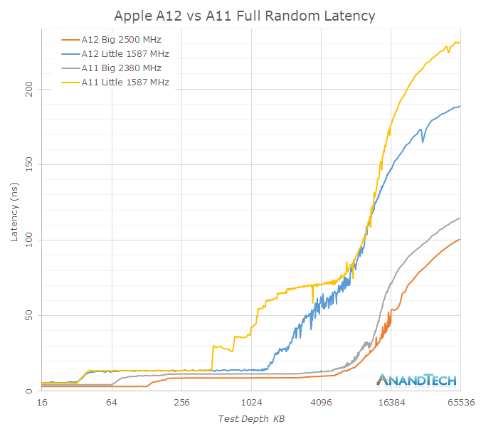
As mentioned in the previous page, it’s evident that Apple has put a significant amount of work into the cache hierarchy as well as memory subsystem of the A12. Going back to a linear latency graph, we see the following behaviours for full random latencies, for both big and small cores:
The Vortex cores have only a 5% boost in frequency over the Monsoon cores, yet the absolute L2 memory latency has improved by 29% from ~11.5ns down to ~8.8ns. Meaning the new Vortex cores’ L2 cache now completes its operations in a significantly fewer number of cycles. On the Tempest side, the L2 cycle latency seems to have remained the same, but again there’s been a large change in terms of the L2 partitioning and power management, allowing access to a larger chunk of the physical L2.
I only had the test depth test up until 64MB and it’s evident that the latency curves don’t flatten out yet in this data set, but it’s visible that latency to DRAM has seen some improvements. The larger difference of the DRAM access of the Tempest cores could be explained by a raising of the maximum memory controller DVFS frequency when just small cores are active – their performance will look better when there’s also a big thread on the big cores running.
The system cache of the A12 has seen some dramatic changes in its behaviour. While bandwidth is this part of the cache hierarchy has seen a reduction compared to the A11, the latency has been much improved. One significant effect here which can be either attributed to the L2 prefetcher, or what I also see a possibility, prefetchers on the system cache side: The latency performance as well as the amount of streaming prefetchers has gone up.
Instruction throughput and latency
| Backend Execution Throughput and Latency | ||||||||
| Cortex-A75 | Cortex-A76 | Exynos-M3 | Monsoon | Vortex | |||||
| Exec | Lat | Exec | Lat | Exec | Lat | Exec | Lat | |
| Integer Arithmetic ADD |
2 | 1 | 3 | 1 | 4 | 1 | 6 | 1 |
| Integer Multiply 32b MUL |
1 | 3 | 1 | 2 | 2 | 3 | 2 | 4 |
| Integer Multiply 64b MUL |
1 | 3 | 1 | 2 | 1 (2x 0.5) |
4 | 2 | 4 |
| Integer Division 32b SDIV |
0.25 | 12 | 0.2 | < 12 | 1/12 - 1 | < 12 | 0.2 | 10 | 8 |
| Integer Division 64b SDIV |
0.25 | 12 | 0.2 | < 12 | 1/21 - 1 | < 21 | 0.2 | 10 | 8 |
| Move MOV |
2 | 1 | 3 | 1 | 3 | 1 | 3 | 1 |
| Shift ops LSL |
2 | 1 | 3 | 1 | 3 | 1 | 6 | 1 |
| Load instructions | 2 | 4 | 2 | 4 | 2 | 4 | 2 | |
| Store instructions | 2 | 1 | 2 | 1 | 1 | 1 | 2 | |
| FP Arithmetic FADD |
2 | 3 | 2 | 2 | 3 | 2 | 3 | 3 |
| FP Multiply FMUL |
2 | 3 | 2 | 3 | 3 | 4 | 3 | 4 |
| Multiply Accumulate MLA |
2 | 5 | 2 | 4 | 3 | 4 | 3 | 4 |
| FP Division (S-form) | 0.2-0.33 | 6-10 | 0.66 | 7 | >0.16 | 12 | 0.5 | 1 | 10 | 8 |
| FP Load | 2 | 5 | 2 | 5 | 2 | 5 | ||
| FP Store | 2 | 1-N | 2 | 2 | 2 | 1 | ||
| Vector Arithmetic | 2 | 3 | 2 | 2 | 3 | 1 | 3 | 2 |
| Vector Multiply | 1 | 4 | 1 | 4 | 1 | 3 | 3 | 3 |
| Vector Multiply Accumulate | 1 | 4 | 1 | 4 | 1 | 3 | 3 | 3 |
| Vector FP Arithmetic | 2 | 3 | 2 | 2 | 3 | 2 | 3 | 3 |
| Vector FP Multiply | 2 | 3 | 2 | 3 | 1 | 3 | 3 | 4 |
| Vector Chained MAC (VMLA) |
2 | 6 | 2 | 5 | 3 | 5 | 3 | 3 |
| Vector FP Fused MAC (VFMA) |
2 | 5 | 2 | 4 | 3 | 4 | 3 | 3 |
To compare the backend characteristics of Vortex, we’ve tested the instruction throughput. The backend performance is determined by the amount of execution units and the latency is dictated by the quality of their design.
The Vortex core looks pretty much the same as the predecessor Monsoon (A11) – with the exception that we’re seemingly looking at new division units, as the execution latency has seen a shaving of 2 cycles both on the integer and FP side. On the FP side the division throughput has seen a doubling.
Monsoon (A11) was a major microarchitectural update in terms of the mid-core and backend. It’s there that Apple had shifted the microarchitecture in Hurricane (A10) from a 6-wide decode from to a 7-wide decode. The most significant change in the backend here was the addition of two integer ALU units, upping them from 4 to 6 units.
Monsoon (A11) and Vortex (A12) are extremely wide machines – with 6 integer execution pipelines among which two are complex units, two load/store units, two branch ports, and three FP/vector pipelines this gives an estimated 13 execution ports, far wider than Arm’s upcoming Cortex A76 and also wider than Samsung’s M3. In fact, assuming we're not looking at an atypical shared port situation, Apple’s microarchitecture seems to far surpass anything else in terms of width, including desktop CPUs.


253 Comments
View All Comments
peevee - Monday, October 15, 2018 - link
"we see four new smaller efficiency cores named “Mistral”. The new small cores bring some performance improvements, but it’s mostly in terms on power and power efficiency where we see Tempest make some bigger leaps"So, is it Tempest or Mistral? Or both?
Ryan Smith - Tuesday, October 23, 2018 - link
It's Tempest. Thanks for the heads up!peevee - Monday, October 15, 2018 - link
"upgrade in sensor size from an area of 32.8mm² to 40.6mm²"These are not sensor sizes, these are total image chip sizes.
Sensor (as in "sensor", the part which actually "senses" light) sizes are not hard to calculate, and are MUCH smaller.
12MP is approx 4000x3000 pixels.
The old sensor had 1.22 µm pixel pitch. 1.22*4=4.88mm. 1.22*3=3.66mm.
So old sensor was 4.88x3.66mm = 17.9mm².
The new sensor is 5.6mm x 4.2mm = 23.5mm².
This is is comparison to
- typical cheap P&S camera sensor size (so-called '1/2.3" type') of 6mm x 4.5mm = 27mm²
- high-end P&S camera sensor, (1" type) of 13.2mm x 8.8mm = 116mm²
- Four Thirds camera sensor size of 17.2 x 13mm = 225mm²
- Modern pro camera sensor size of about 36x24mm = 864mm².
Please do not confuse your readers by calling total image chip sizes as "sensor size".
peevee - Monday, October 15, 2018 - link
"The performance measurement was run in a synthetic environment (read: bench fan cooling the phones) where we assured thermals wouldn’t be an issue for the 1-2 hours it takes to complete a full suite run."Which makes the whole thing useless. Of course wider (read hotter and less efficient due to higher overhead of often-useless blocks) will run faster in this environment, unlike in user hands (literally, ~36C/97F plus blanketing effect).
Andrei Frumusanu - Monday, October 22, 2018 - link
It changes absolutely nothing. It will still reach that performance even in your hands. The duration of a workload is not orthogonal to its complexity.viczy - Sunday, October 21, 2018 - link
Fantastic and in-depth work! Thanks for the data and analysis. I would like to know a little more about your method for energy and power measurement. Thanks!techbug - Friday, November 2, 2018 - link
Thanks a lot Andrei.L2 cache latency is 8.8ns, Core clock speed is 2.5GHz, each cycle is around 0.4ns, then the l2 cache latency is 8.8ns/0.4=22 cycles. This is much longer than Skylake, which is around 12 cycles (taking i7-6700 Skylake 4.0 GHz at https://www.7-cpu.com/cpu/Skylake.html as an example, it equals to 3ns L2 cache latency).
So L2 latency is 8.8ns versus 3ns in skylake. Is this comparison correct?
I cannot tell the precise L1 latency from the graph "Much improved memory latency". Can you give the number?
According to Figure 3 in https://www.spec.org/cpu2006/publications/SIGARCH-... the working set size of 80% SPEC2K6 workload is larger than 8MB, A12 's L2 cache (8MB) won't hold the working set. Compared with 32MB L3 cache Skylake configuration.
So overall the memory hierarchy of A12 seems not comparable to Skylake. What else helps it to deliver a comparable SPEC2K6 performance?
demol3 - Wednesday, December 5, 2018 - link
Will there be a comparison between XS-series and XR or XR review anytime soon?tfouto - Thursday, December 27, 2018 - link
Does XS has a true 10-bit panel, or uses Frame Rate Control?What about Iphone X?
Latiosxy - Wednesday, January 23, 2019 - link
Hello. I just wanted to criticize the way this site works. It’s hard to read while listening to music when your intrusive ads follow my screen and interrupt my audio consistently. Please fix this as this has been really annoying. Thanks.