Qualcomm Launches Snapdragon Wear 3100 Platform for Smartwatches
by Anton Shilov on September 14, 2018 11:15 AM EST- Posted in
- SoCs
- Snapdragon
- Qualcomm
- Wearables
- Snapdragon Wear
Qualcomm this week introduced its new platform designed for smartwatches based on Google’s Wear OS. The long anticipated Snapdragon Wear 3100 packs four general-purpose processing cores as well a special co-processor for low-power operations designed to prolong battery life of upcoming wearables. Communication capabilities of the platform include GPS, Wi-Fi+Bluetooth, as well as 4G/LTE, which is in line with features supported by direct predecessor.
Qualcomm’s Snapdragon Wear 3100 (MSM8909w) is the company’s most powerful SoC for wearables that the company has released to date. Just like the Snapdragon Wear 2100 introduced in 2016, the new chip packs four ARM Cortex-A7 cores clocked at 1.2 GHz. Meanwhile, the latest SoC also integrates the company’s QCC1110 co-processor designed specifically for tasks that do not require serious compute horsepower, such as sensor processing in new modes to be supported by the upcoming version of Wear OS. The co-processor also has a deep learning engine for custom workloads like detection of keywords.
Besides general-purpose cores and the co-processor, the SoC integrates Qualcomm’s Adreno 304 GPU that supports resolutions up to 640x×480 at 60 Hz as well as a high-performance DSP. As for communication capabilities, the Snapdragon Wear 3100 platform can support Qualcomm’s WCN3620 Wi-Fi/Bluetooth controller, Qualcomm’s Snapdragon X5 4G/LTE modem, and GPS capabilities. Meanwhile, the company will offer three versions of the SW3100 targeting smartwatches with different comm features.
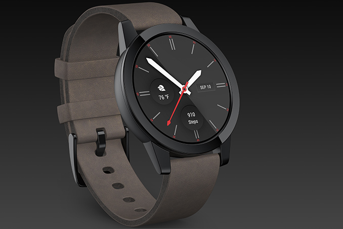
Qualcomm says that it works closely with developers of Google’s Wear OS, so all the capabilities of the new Snapdragon Wear 3100 platform will be used by software eventually. In particular, the SW3100 will support three modes that will be a part of next-gen watches running the Wear OS, including the Enhanced Ambient Mode, Dedicated Sports Experiences, and Traditional Watch Mode. In all three cases the SW3100 will offload display and sensor processing from the Cortex-A7 and Adreno cores to the ultra-low-power co-processor, but will still be able to perform typical tasks for each mode (e.g., GPS and heart rate sensing for the sports mode).
| Qualcomm Snapdragon Wear SoCs | ||||
| Snapdragon Wear 1200 | Snapdragon Wear 1100 | Snapdragon Wear 2100 | Snapdragon Wear 3100 | |
| SoC | Cortex-A7 @ 1.3GHz Fixed-function GPU |
Cortex-A7 @ 1.2GHz Fixed-function GPU |
4x Cortex-A7 @ 1.2GHz Adreno 304 |
4x Cortex-A7 @ 1.2GHz QCC1110 co-processor Adreno 304 |
| Process Node | 28nm LP | 28nm LP | 28nm LP | ? |
| RAM | LPDDR2 | LPDDR2 | LPDDR3-800 MT/s | LPDDR3 (?) |
| Display | Simple 2D UI | Simple 2D UI | Up to 640x480 @ 60fps | |
| Modem | Qualcomm (Integrated) 2G (E-GPRS) / LTE (Cat M1 & Cat NB1) |
Qualcomm (Integrated) 2G / 3G / LTE (Category 1 10/5 Mbps) |
Qualcomm X5 (Integrated) 2G / 3G / LTE (Category 4 150/50 Mbps) Connected version only |
|
| Connectivity | 802.11b/g/n/ac, BT 4.2 LE, GPS/GLONASS/Galileo/BeiDou | 802.11b/g/n/ac, BT 4.1 LE, GPS/GLONASS/Galileo/BeiDou (Wi-Fi and BT optional) |
802.11b/g/n (2.4GHz), BT 4.1 LE, NFC, GPS/GLONASS/Galileo/BeiDou, USB 2.0 Connected and Tethered versions |
|
Qualcomm claims that the QCCC1110 co-processor, the PMW3100 power management sub-system, and other enhancements of the Snapdragon Wear 3100 will help to reduce the SoC's power consumption rather significantly. The net benefit from this, according to Qualcomm, is that device makers will be able to prolong the battery life of their devices by 4 to 12 hours when compared to the previous-generation Snapdragon Wear 2100 platform.
Qualcomm says that mass production of the Snapdragon Wear 3100 had already started, as have shipments to customers. The first companies to adopt the new SoC are Fossil Group, Louis Vuitton, and Montblanc.
As is usually the case for the chip vendor, Qualcomm is not disclosing when their customers intend to release their SW3100-powered watches to consumers. However what we're hearing from other sources is that the first watches should hit store shelves next month, in which case we're looking at a relatively quick turnaround time here.
Related Reading:
- Qualcomm Announces Snapdragon 2500 Wearable Platform For Kids Watches
- Qualcomm Announces Snapdragon Wear 1200 SoC: LTE Categories M1 & NB1 for Wearables & Smart Trackers
- ASUS ZenWatch 3 Announced: Round Display, Snapdragon Wear 2100, Long Battery Life
- Qualcomm Announces Snapdragon Wear 1100 SoC For Wearables
- Qualcomm Announces Snapdragon Wear 2100 IoT SoC
Source: Qualcomm


43 Comments
View All Comments
tipoo - Saturday, September 15, 2018 - link
The A32 is more efficient than the A7, unless you don't think ARM knows about their own cores.The Wear 2100 design was three years old, Qualcomm "knows what they're doing" from an investment standpoint, certainly, but you have blinders on if you don't think this was left to languish, as this chip is barely any different apart from the decent low power core addition.
tipoo - Saturday, September 15, 2018 - link
"It’s the year where I’m right and you’re wrong."Cute, but you acknowledge the opposite later. Your original claim was -
"Yes, clearly smart watches that are still held back by battery capacity need more powerful CPUs chucked at them!"
Then you came around to
"You could get an SOC using even less power on a newer node, but who’s going to pay for it."
Nice moving of the goalposts there. Yes, who is going to pay for it is precisely the issue, but the fact remains that this old chip could have benefitted from a newer node, as I said, and ARM thinks the A32 is more efficient.
tuxRoller - Friday, September 14, 2018 - link
Qualcomm has claimed that the smaller nodes have sufficiently worse static leakage such that it dominates the typical usage pattern.Gadgety - Saturday, September 15, 2018 - link
I've seen that claim, but no numbers are presented. It may be true for Qualcomm's processors. Then again I wonder why does Samsung use smaller nodes in their wareables? They also have great battery life compared to the current Wear devices. This may be influenced by Tizen possibly being more efficient than Wear OStipoo - Saturday, September 15, 2018 - link
I remember that around the 20nm half node, but 14nm certainly seemed like a win on all fronts, let alone 7.Death666Angel - Friday, September 14, 2018 - link
Any modern manufacturing mode would reduce power consumption of the SoC. And I'd guess that a nice A53 or A55 would be more efficient than an A7 as well. Both are still in-order architectures and have IPC gains that can be translated to better clock/V states. It's rare that an outdated architecture on an outdated manufacturing node is competitive in anything, let alone efficiency.V900 - Friday, September 14, 2018 - link
And that’s where you’d be wrong.The Cortex A7 is more energy efficient than the A53 by quite a margin if you’re talking about a device as starved power as a watch.
Look at this test from Anandtech for example: https://www.anandtech.com/show/8718/the-samsung-ga...
Raqia - Friday, September 14, 2018 - link
Leakage current of whatever 28nm process Qualcomm is using is better than smaller nodes:https://www.androidpolice.com/2018/09/10/qualcomm-...
"Even the fact that the chipset is built on a 28nm fabrication node (which hasn't been cutting edge technology since 2013), comes down to power savings, according to Qualcomm. Since smaller nodes are generally known for being more power efficient (either that, or a lot more powerful), that may seem somewhat contradictory. But Qualcomm told Android Police it chose not to shrink the process node because the passive drain on a 10nm process is significantly higher than 28nm, and a smartwatch is in idle mode the majority of its time in use. Of course, a 28nm fabrication process is no doubt also less expensive than 10nm, so perhaps that played into the decision, though we can't know for sure."
And this makes sense for watches which are predominantly going to be idle.
Most of what a 64 bit CPU would offer would be wider pointers which even Apple isn't really using:
https://www.anandtech.com/show/13364/apple-announc...
"It’s to be noted that the 64-bit part of the new CPU might not be as clear as one might think, as there’s been some evidence (Credit @KhaosT) that the Watch might be running in ARM64_32 mode, which would be a 32-bit submode of AArch64 that allows for 32-bit pointers while retaining the ISA advantages of AArch64. Such a mode would be most optimal for a low-memory device such as smartwatch."
There are some advantages to ARM-V8 besides more addressable memory, but I imagine Apple more or less wanted the CPU design to be in-house and to have some redundancy with its phone designs first rather than 64 bit for any inherent advantages it would offer watch software.
name99 - Friday, September 14, 2018 - link
ILP32 is not a "CPU" mode, it is a compiler model. It's part of LLVM, and Android could use it for Android Wear if they wanted; to pick up the efficiency benefits of the ARMv8 64-bit ISA, while not paying the RAM costs.But of course for that to happen would require all the various parties (Google, QC, watch makers) to get their act together and actually give a damn about shipping a competitive product. They seem utterly uninterested in doing that...
Meanwhile it's simply not true that "no-one buys smart watches". Apple is probably (all we have is estimates, so we can't be absolutely sure) the largest watch company in the world by both units shipped and revenue. In 2017 they were shipping a million a month. Best guess is this is now a million every fortnight. With Series 4, it'll probably soon be a million a week.
name99 - Friday, September 14, 2018 - link
So I guess it's now confirmed. Anand Chandrasekher's AnandTech name is V900!Remember these wise words when the iPhone 5S was released:
“I think they are doing a marketing gimmick. There’s zero benefit a consumer gets from that”