HiSilicon Announces The Kirin 980: First A76, G76 on 7nm
by Andrei Frumusanu on August 31, 2018 8:30 AM EST- Posted in
- Mobile
- Smartphones
- SoCs
- HiSilicon
- 7nm
- Cortex-A76
- Mali-G76
- Kirin 980
This year at IFA, instead of suddenly finding the new silicon on the show floor, Huawei’s CEO Richard Yu announced this year’s new Kirin 980 during the company’s keynote speech. For readers who’ve been attentively following our articles over the last few months, today’s news should hopefully not come at too big of a surprise, as I’ve been heavily hinting at the timing of the first new 7nm Cortex A76 silicon designs coming later this year in commercial devices, with HiSilicon being the prime candidate for being the first vendor on the market with the their new generation SoC.
Huawei’s silicon design division HiSilicon has been a key strategic component for the company’s products, as it enables it to differentiate itself in a more drastic way than what we usually see from other vendors who simply rely on established open-market SoC vendors such as Qualcomm. This kind of strategy of course is a double-edged sword, as if you’re all-in with your in-house silicon, it also means that these designs must be executed properly, as otherwise you find yourself in an unfavourable competitive position.
The Kirin 950 was an impressive chip as it boasted the first Cortex A72 design on a then new TSMC 16FF manufacturing process – this paid off plenty for Huawei as the combination of new IP as a new manufacturing node resulted in a very competitive silicon which directly translated into favourable characteristics of the handsets in that it was used in.
The Kirin 960 and Kirin 970 on the other hand showcased the risky side of this strategy, and where things can go off-track – the Kirin 960 was a 16nm SoC released in a device generation where 10nm competitors such as the Snapdragon 835 and Exynos 8895 dominated. The Kirin 970 fared better when switching to a 10nm manufacturing node, but this time around HiSilicon wasn’t able to include the newest Arm CPU IP, relying on an A73 CPU while the Snapdragon 845 embraced the new A75. Furthermore the last two Kirin generations had showcased extremely uncompetitive GPU performance and efficiency figures – here HiSilicon is stuck and is at the whim of IP vendors’ ability to produce competitive designs against market leaders such as Qualcomm.
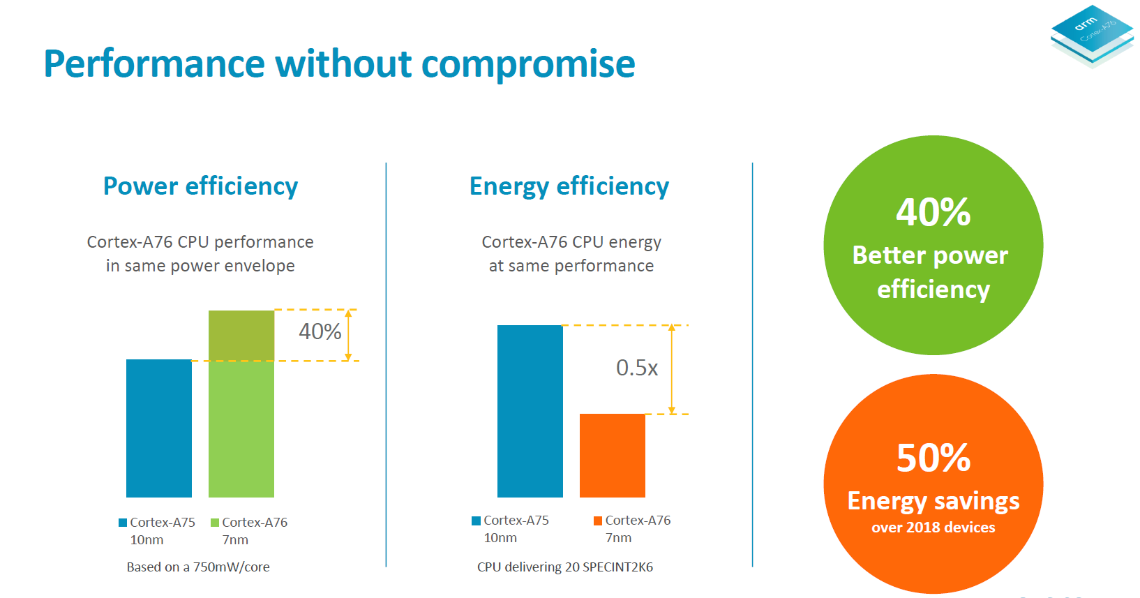
The reason as to why I reiterated what happened to the last few generations, is that this time around HiSilicon finds itself in a very favourable position where IP and manufacturing is aligned into what is essentially a best-case scenario for the new design. Arm’s new Cortex A76 and Mali G76 both promise great leaps in terms of performance and power efficiency, and TSMC is in mass production of its new 7nm manufacturing node.
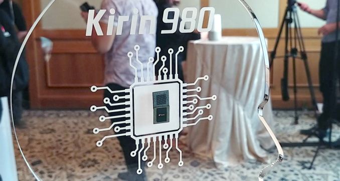
Today we present the new Kirin 980, the first announced TSMC 7nm SoC as well as the first Cortex A76 and Mali G76 design:
| HiSilicon High-End Kirin SoC Lineup | |||
| SoC | Kirin 980 | Kirin 970 | Kirin 960 |
| CPU | 2x A76 @ 2.60 GHz 2x A76 @ 1.92 GHz @ 512KB L2's 4x A55 @ 1.80 GHz @ 128KB L2's 4MB DSU L3 |
4x A73 @ 2.36 GHz 4x A53 @ 1.84 GHz 2MB L2 |
4x A73 @ 2.36GHz 4x A53 @ 1.84GHz 2MB L2 |
| GPU | ARM Mali-G76MP10 @ 720 MHz |
ARM Mali-G72MP12 @ 746 MHz |
ARM Mali-G71MP8 @ 1037MHz |
| LPDDR4 Memory |
4x 16-bit CH LPDDR4X @ 2133MHz 34.1GB/s |
4x 16-bit CH LPDDR4X @ 1833 MHz 29.9GB/s |
4x 16-bit CH LPDDR4 @ 1866MHz 29.9GB/s |
| Storage I/F | UFS 2.1 | UFS 2.1 | UFS 2.1 |
| ISP/Camera | New Dual ISP +46% speed 10-bit pipeline |
Dual 14-bit ISP | Dual 14-bit ISP (Improved) |
| Encode/Decode | 2160p60 Decode 2160p30 Encode :( |
2160p60 Decode 2160p30 Encode |
1080p H.264 Decode & Encode 2160p30 HEVC Decode |
| Integrated Modem | Kirin 980 Integrated LTE (Category 21/18) DL = 1400 Mbps 4x4 MIMO 3x20MHz CA, 256-QAM (5CA no MIMO) UL = 200 Mbps 2x2 MIMO 1x20MHz CA, 256-QAM |
Kirin 970 Integrated LTE (Category 18/13) DL = 1200 Mbps 5x20MHz CA, 256-QAM UL = 150 Mbps 2x20MHz CA, 64-QAM |
Kirin 960 Integrated LTE (Category 12/13) DL = 600Mbps 4x20MHz CA, 64-QAM UL = 150Mbps 2x20MHz CA, 64-QAM |
| Sensor Hub | i8 | i7 | i6 |
| NPU | Dual @ >2x perf | Yes | No |
| Mfc. Process | TSMC 7nm | TSMC 10nm | TSMC 16nm FFC |
The new Kirin 980 checks off all of the newest available IPs from Arm, finally employing a new DynamIQ CPU cluster configuration comprised of 4 Cortex A76's and 4 Cortex A55s.
The biggest surprise to today’s announcement for me is to see that HiSilicon has made the step forward to fully take advantage of Arm’s new DSU cluster and its asynchronous CPU configuration, and actually implement the brand new Cortex A76 into two groups, each housed in their own clock and voltage plane.
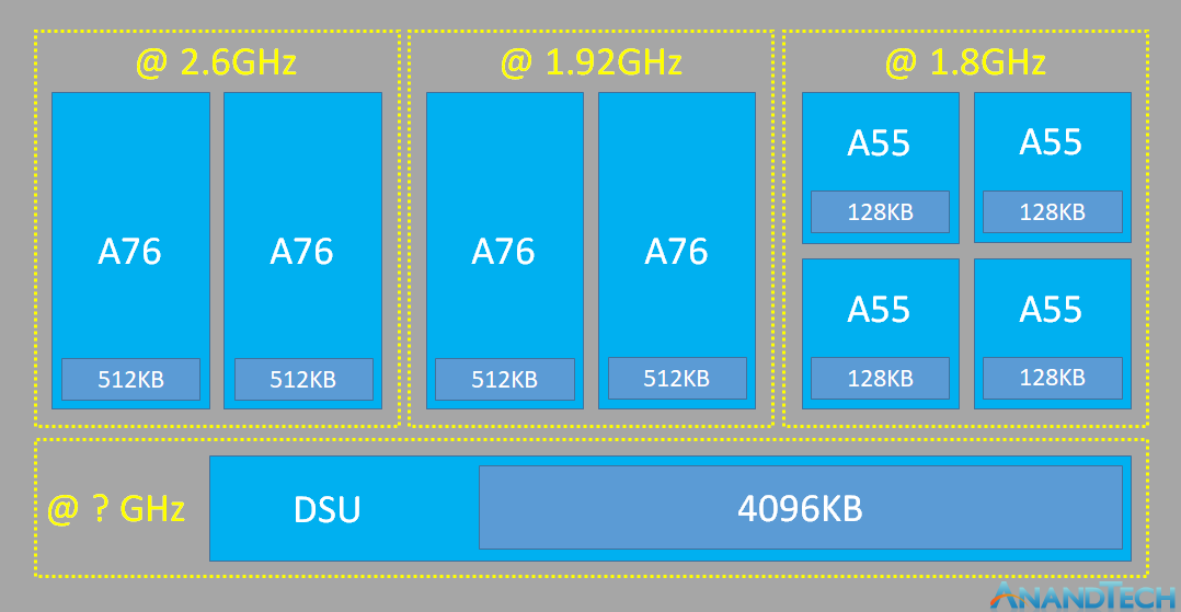
The highest performance Cortex A76 pair runs at up to 2.6GHz. This is less than Arm’s originally announced 3GHz target for the CPU, however I had warned readers to expect more conservative clocks around the 2.5GHz figure, as the higher clock rates seemingly were meant for higher TDP form-factors. Nevertheless, the new CPU microarchitecture still brings with it substantial performance improvements, and thus will still perform very well at 2.6GHz, posting leading performance for this generation.
The surprise of seeing the second pair of Cortex A76 cores running at up to 1.92GHz is actually quite fantastic news for power efficiency. Here we see HiSilicon include what is essentially a “medium” efficiency group of CPUs. Because these two cores are running on a separate clock and voltage plane to the primary performance A76 pair, it means they can operate at different efficiency points, enabling more effective power savings in varied multi-threaded operation.
Previously, quad-core clusters were running on the same clock and voltages, and if there was a single high performance thread requiring a high performance state, it meant that other medium-performance threads were forced to take a power efficiency penalty by needlessly running at this less efficient performance state. By introducing a mid-tier, this effectively eliminates such kind of overhead which is commonly found in real-world applications.
I haven’t been able to confirm this with HiSilicon as of yet, but the reduced clock of this mid pair of A76 would also strongly point out to a possibly different physical implementation with a lower silicon sign-off frequency. This means that even though both pairs of A76’s are the same IP, this mid-pair are very likely to actually be more efficient when running at the same frequency.
Finally, we see four new Cortex A55 cores as the most power-efficient workhorses of the SoC who’ll be able to take the brunt of workloads, running at up to 1.8GHz. Here again, virtue of the mid-performance cluster, HiSilicon is likely able to implement a very power-efficiency focused physical implementation for the A55’s, resulting in clock speeds that in range with current generation A53 and A55 SoCs.
Cache wise, all the Cortex A76’s come with their recommended 512KB L2 cache configurations while the A55’s employ 128KB caches. As a reminder, in the new DynamIQ cluster configuration, the L2 caches for these designs are private to each CPU core. The L3 cache in the DSU has seen a full implementation at 4MB, double that of what we’ve seen in the Snapdragon 845.
I haven’t been able to confirm the frequency of the DSU in the Kirin 980, nor if it actually has a separate clock and voltage plane of its own, here it might be possible that it’s could be on the same plane with the A55’s. Again, that’s just speculation on my part, the other possibility is that we have 4 full clock and voltage planes for the whole CPU complex.
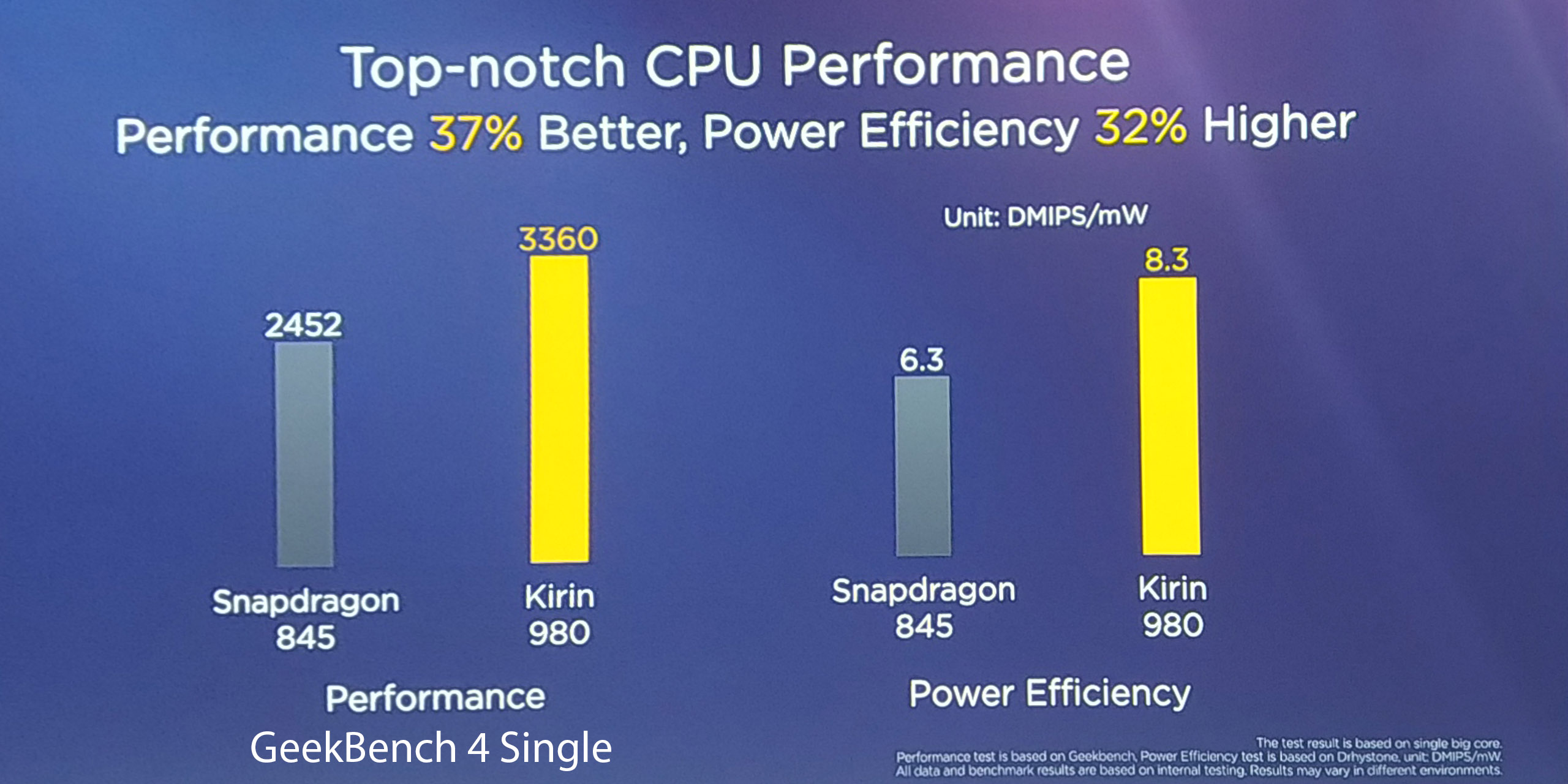
75% higher CPU performance, 58% better efficiency compared to Kirin 970
In terms of performance gains, HiSilicon promises 75% gains over the Kirin 970, which after a bit of math actually ends up basically exactly where I had projected the A76 to land, based on Arm’s own performance claims.
The following projection is of my own, and takes into account both Arm’s and HiSilicon’s matching performance claims:
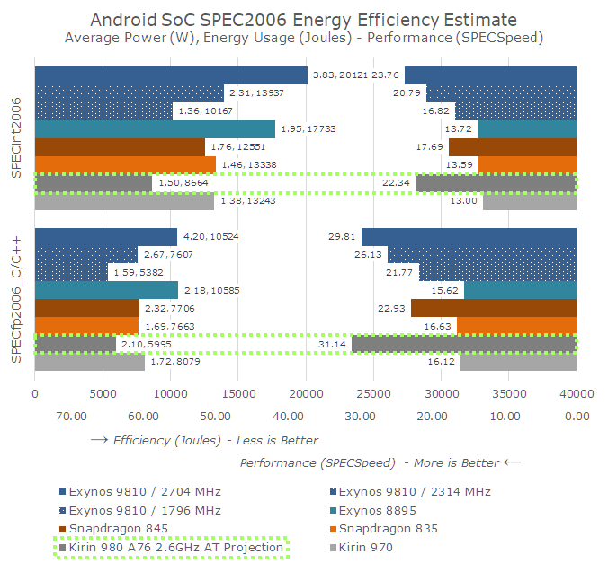
As you may have noted, the power and efficiency estimates are also included. HiSilicon proclaims that the Kirin 980 is 58% more power efficient than the Kirin 970. We haven’t been able to clarify if this means that the perf/W is 58% better at the same performance of the 970, or if the Kirin 980 has a 58% better perf/W at both SoC’s respective peak performance states. The projection assumes the latter, and it actually again it matches up with Arm’s own claims about the Cortex A76.
I’m still very very sceptical about these numbers as they seem quite fantastic; yet to date I haven’t seen any contradictory information that would actually rebuke these estimates. For the time being, until we actually get our hands on the first Kirin 980 device, take the above power and efficiency estimate with a large grain of salt.
Update Post-Keynote: During the presentation Huawei’s footnotes clarified that the efficiency figures are based on Dhrystone. Dhrystone is very CPU core enclosed and doesn’t stress the rest of the SoC nearly as much in terms of memory traffic, putting some doubts into the above estimates as well as Huawei’s power figures.
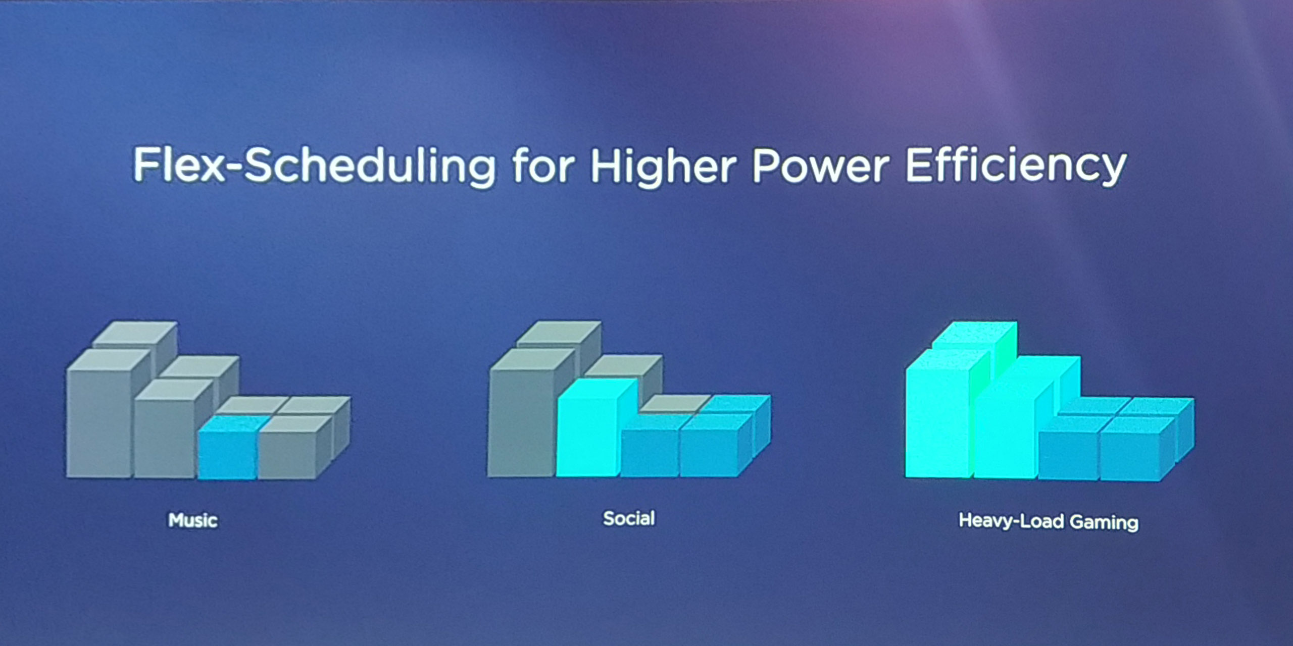
The move to a 3-tier CPU hierarchy also brings with itself complications in terms of scheduling. As we’ve seen this year, scheduling is very much a new critical component of modern SoCs as with the very high dynamic range of performance and power, using the most optimal solution is critical in extracting the best out of the silicon. Here HiSilicon promises a new “Flexible scheduling” mechanism. We unfortunately don’t have any more details on this, but it’s going to be a crucial component of the new Kirin 980.


120 Comments
View All Comments
melgross - Friday, August 31, 2018 - link
Do you really think that this will be the first smartphone SoC shipped in a product? It seems that Apple will have a good claim on that. Or do you just not want to mention a non Android, non AOSP product? While we won’t know for certain which cores they will use, it’s not important, because whichever they choose will be highly modified anyway.Achtung_BG - Friday, August 31, 2018 - link
Pls more info for Balong 5000 and 5G technology.Andrei Frumusanu - Friday, August 31, 2018 - link
I added a paragraph under the modem bit, unfortunately we don't have any more info on that part.centurio9 - Friday, August 31, 2018 - link
Can't wait to see it next year in some ~400$ Honor device :DZolaIII - Friday, August 31, 2018 - link
Hmm... "though both pairs of A76’s are the same IP, this mid-pair are very likely to actually be more efficient when running at the same frequency" I don't think so. It depends on power rails implemented but it's still both more costly and uter stupid to implement two areas of them for four core's instead implementing one with cuple more rails. Future on it's also utterly stupid to implement mid tier CPU core's along with developing (property) scheduler for them instead just making a hand brake based on relative utilisation (in two points; optimal & sustainable frequency).Come on now? 178% more power efficient. What it sips 3W into battery when pushed hard. 100% less than something is zero.
Two huge not optimized for application use NNPU's. That must be a new record in black silicone on any mobile SoC. I am still for the DSP's that are also optimised for NNPU task's. At least that way we would see a benefit in the multimedia capabilities.
Another rather bad design regarding me. At least how it looks like this time around they will improve regarding GPU capabilities and power consumption.
Andrei Frumusanu - Friday, August 31, 2018 - link
I have no idea what you're trying to say regarding the A76s. The two pairs are on their own voltage rails. If you're TDP limited in a quad-design, then clocking down a pair of them and putting them on a separate rail is only beneficial.178% better perf/W, it's a growing figure. The estimates check out.
NPUs have their place as dedicated silicon, you need to be able to run imaging and inferences alongside each other. That can't be done with just one DSP. The Kirin 970 already had a Cadence DSP of similar capability of what you see in Snapdragons - alongside the NPU. The 980 won't be any different.
Wardrive86 - Friday, August 31, 2018 - link
I was under the assumption that Cadance had not implemented floating point support (fixed point only) or SMT in their DSPs. They have very performant DSPs, I don't question that..but not quite to the level of the QDSP6v6. Last I checked they were falling short of QDSP6v5 after they introduced DMT. Unfortunately Cadence doesn't rely on BDTI so reliable benchmarks are hard to come by.ZolaIII - Friday, August 31, 2018 - link
Think you didn't bean following the DSP scene for a very long time.Wardrive86 - Friday, August 31, 2018 - link
I am very up to date in regards to the DSPs that immediately "matter" to me Hexagon 400-600 series and also many CEVA DSPs. Admittedly it can be difficult to keep up with all of them. I do see they added support as of 2017. It seems the C5, Q6 and P6 are geared towards vision and AI applications, but doesn't seem to be a multithreaded architecture the way that Hexagon is. So I agree you would need a NPU if you were using one of their DSPs, the same is not true of HexagonZolaIII - Friday, August 31, 2018 - link
I am trying to say about mid pair of the A76's how they are just another waist of silicon & will slow things down additionally. I am for just a pair of big cores. It's smarter to put only a pair of them add more power rails & limit their up scaling based on high utilisation on let's say 1.6GHz & 2GHz. You save on silicon & they don't have penalty of another migration, you also save on DTP they use as you know they use a lot even while only idling. Would be good if we could also limit SMP tasks that can use more than two core's only on smal in order one's & trow in more of those (small core's).I figured out for what 178% figure stands for but I have hard time believing it all together how G76 will be 78% faster per/W. 70% is my best educated guess & still per cluster. But we will see that only when we get silicone.
Now look at it this way. NNPU on the Kirin 970 whose huge chuck of silicone that we didn't use to often & it whose really bad design (with out ¼ precision). It looks like they didn't do anything regarding improving design and they are now pushing two of those. Really? For me that is as bad as it can get. I never mentioned neither only one nor MP1 DSP's nor most modern ADSP's are single threaded. I am not against NN just against specialised single purpose accelerators on the SoC's with both limited DTP & price point. As we simply can't put in big enough FPGA (or EFPGA) to be useful I think program-able DSP adopted for NN are best match. Putting even two MP4 Tensilica DSP's would eat lot less silicone while being much more useful & still good enough for NN tasks. We will talk more when you do a Mate review.