HiSilicon Announces The Kirin 980: First A76, G76 on 7nm
by Andrei Frumusanu on August 31, 2018 8:30 AM EST- Posted in
- Mobile
- Smartphones
- SoCs
- HiSilicon
- 7nm
- Cortex-A76
- Mali-G76
- Kirin 980
New Mali G76MP10: Actually 20 "rendering pipelines"
Moving on, the Kirin 980 is also the first SoC to employ Arm’s new generation Mali G76 GPU. The G76 greatly differs from past Midgard and Bifrost GPUs in that it vastly changes the block structure inside what you consider a “core”. Here the G76 essentially doubled up on texture units, render units, and doubles the width of the arithmetic pipelines. In effect, a G76 core is pretty much equivalent to two G72 cores.
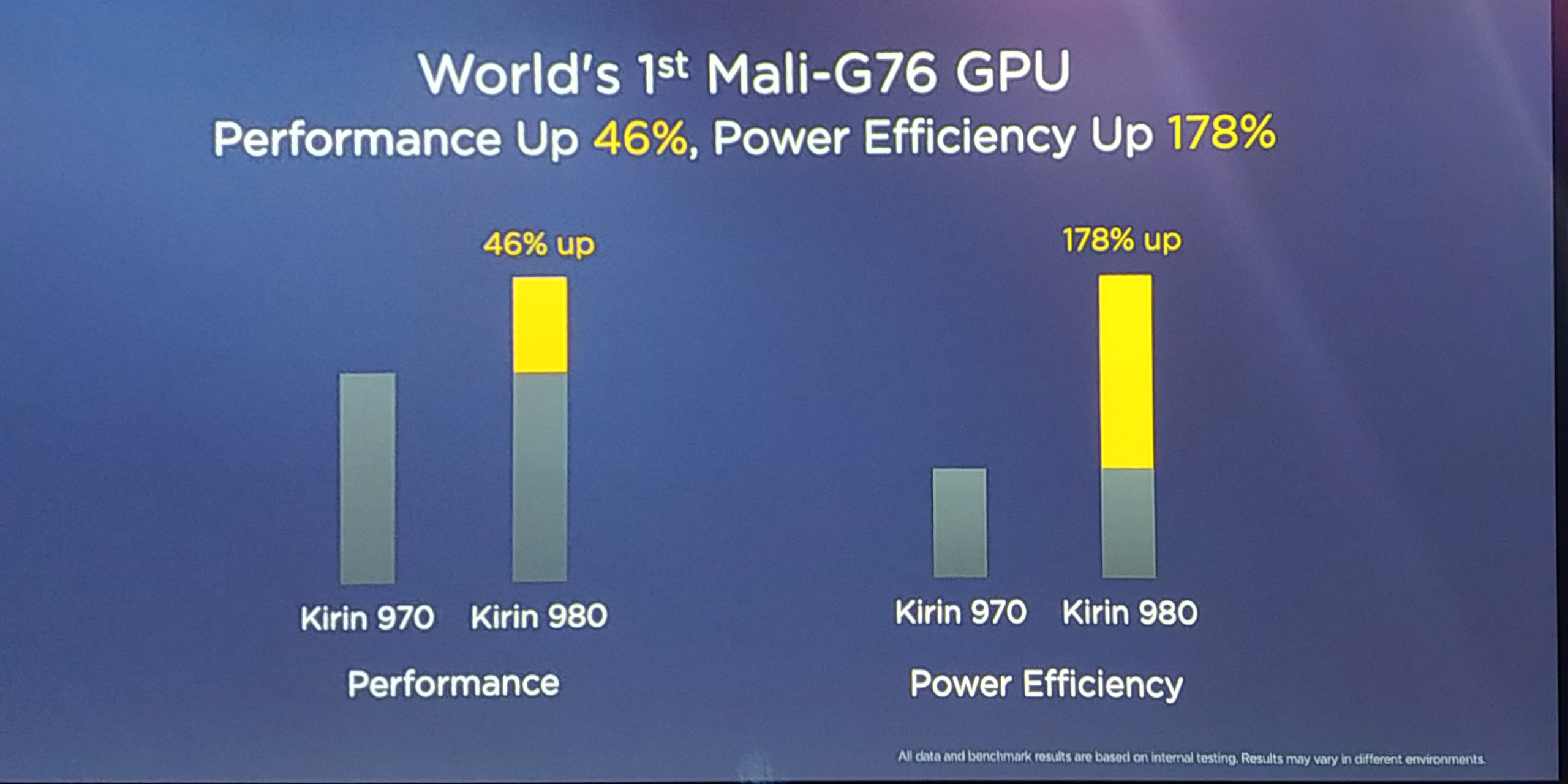
What this means that while on paper the G76MP10 might at first glance looks smaller than the G72MP12 in the Kirin 970, yet it actually represents a 66% increase in the computational resources, not taking into account microarchitectural improvements of the new IP.
The Kirin 970’s GPU was clocked at up to 747MHz – however the power draw at this frequency was still too great for the SoC to handle, resulting in real-world workloads effectively running at much lower frequencies.
The Kirin 980 runs the new GPU at 720MHz and promises a 46% performance boost. We didn’t have any clarification of the workload here, but generally the industry standard is usually GFXBench Manhattan.
46% higher performance, and *178%* higher power efficiency
Now the real kicker of the new GPU, is that HiSilicon proclaims a massive 178% boost in power efficiency when compared to the Kirin 970. Putting these claims into our efficiency table and extrapolating the results:
| GFXBench Manhattan 3.1 Offscreen Power Efficiency (System Active Power) |
||||
| Mfc. Process | FPS | Avg. Power (W) |
Perf/W Efficiency |
|
| Kirin 980 Projection Based on +% | 7FF | 55 ? | 3.5 ? | 16 fps/W ? |
| Galaxy S9+ (Snapdragon 845) | 10LPP | 61.16 | 5.01 | 11.99 fps/W |
| Galaxy S9 (Exynos 9810) | 10LPP | 46.04 | 4.08 | 11.28 fps/W |
| Galaxy S8 (Snapdragon 835) | 10LPE | 38.90 | 3.79 | 10.26 fps/W |
| LeEco Le Pro3 (Snapdragon 821) | 14LPP | 33.04 | 4.18 | 7.90 fps/W |
| Galaxy S7 (Snapdragon 820) | 14LPP | 30.98 | 3.98 | 7.78 fps/W |
| Huawei Mate 10 (Kirin 970) | 10FF | 37.66 | 6.33 | 5.94 fps/W |
| Galaxy S8 (Exynos 8895) | 10LPE | 42.49 | 7.35 | 5.78 fps/W |
| Galaxy S7 (Exynos 8890) | 14LPP | 29.41 | 5.95 | 4.94 fps/W |
| Meizu PRO 5 (Exynos 7420) | 14LPE | 14.45 | 3.47 | 4.16 fps/W |
| Nexus 6P (Snapdragon 810 v2.1) | 20Soc | 21.94 | 5.44 | 4.03 fps/W |
| Huawei Mate 8 (Kirin 950) | 16FF+ | 10.37 | 2.75 | 3.77 fps/W |
| Huawei Mate 9 (Kirin 960) | 16FFC | 32.49 | 8.63 | 3.77 fps/W |
| Huawei P9 (Kirin 955) | 16FF+ | 10.59 | 2.98 | 3.55 fps/W |
The proclaimed performance boost would still be a tad too low catch up to the Snapdragon 845’s Adreno 630, at least in this workload. Here depending on how the Mali G76 scales, we might have different results based on different tests, showing a rebalancing of fillrate heavy workloads versus arithmetic/compute heavy workloads.
Where the Kirin 980 would showcase a large jump is in power consumption and efficiency. Again, HiSilicon’s marketing claims here end up matching what we had projected for the G76, based on Arm’s own figures. If this ends up as expected in measured devices, it would mean that the new Kirin would finally get back to sustainable power levels of that of the Kirin 950, shedding away the awful legacy of the first two Bifrost generation GPUs.
I’ve been banging the drums of the problem of sustainable performance a lot this year, and I do really hope the Kirin 980 ends up near the projections, because that would be a significant step forward for not only the SoC, but general consumer experience as well.
Faster memory controller
The new chipset sports an LPDDR4X memory controller, although it’s able to claim to be the industry’s first one to run at 2133MHz, resulting in a 13% increase in bandwidth. One of the weaknesses of the Kirin 970 was a memory controller that was quite power hungry at higher frequencies, here’s to hoping that the new design resolves these issues and we see better efficiency at high performance states.
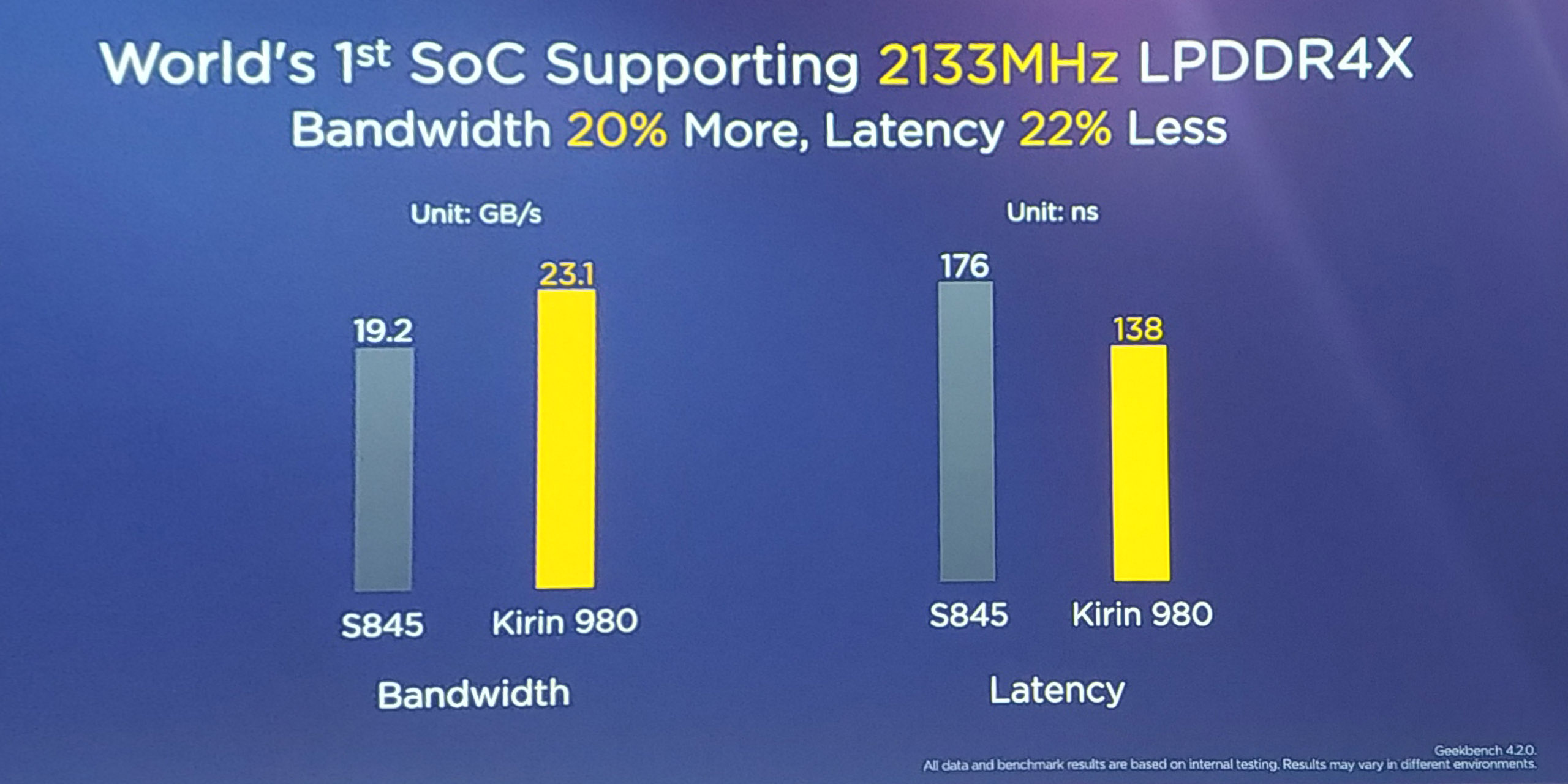
Surprisingly, HiSilicon disclosed some memory latency and bandwidth figures: In the GeekBench 4 tests the Kirin 980 measures 138ns versus a quoted 176ns for the Snapdragon 845. This actually was a bit eye-brow raising as in context, the latency figure isn’t all that good: the Kirin 970 sported a similar 138ns latency as well, coming in the same ballpark of the Snapdragon 835. Yet all are worse than the Exynos 9810’s 78ns figure. There are some inaccuracies with GB4's test here in terms of absolute figures, but in general the ranking between the platforms is still correct. Here I do hope the non-improvement doesn’t limit the peak performance of the A76 in the same way Qualcomm’s added latency of their new L4 system cache in the S845 hindered the A75 core’s performance.
Bandwidth figures are quoted at 23.1GB/s versus 19.2GB/s for the Snapdragon 845. I’ve been told GB4’s memory bandwidth test has issues scaling up after a certain point, so I’m not putting too much weight on these results for the time being.
New ISP with imaging features
The Kirin 980 sports a new ISP that increases is processing throughput capability by up to 46%, able support higher resolution camera streams. A first for HiSilicon is the introduction of a 10-bit pipeline for HDR capture, a feature also introduced in this year's competing SoCs, however only seldom used in practise due to colour management and displays lagging behind in terms of adoption.
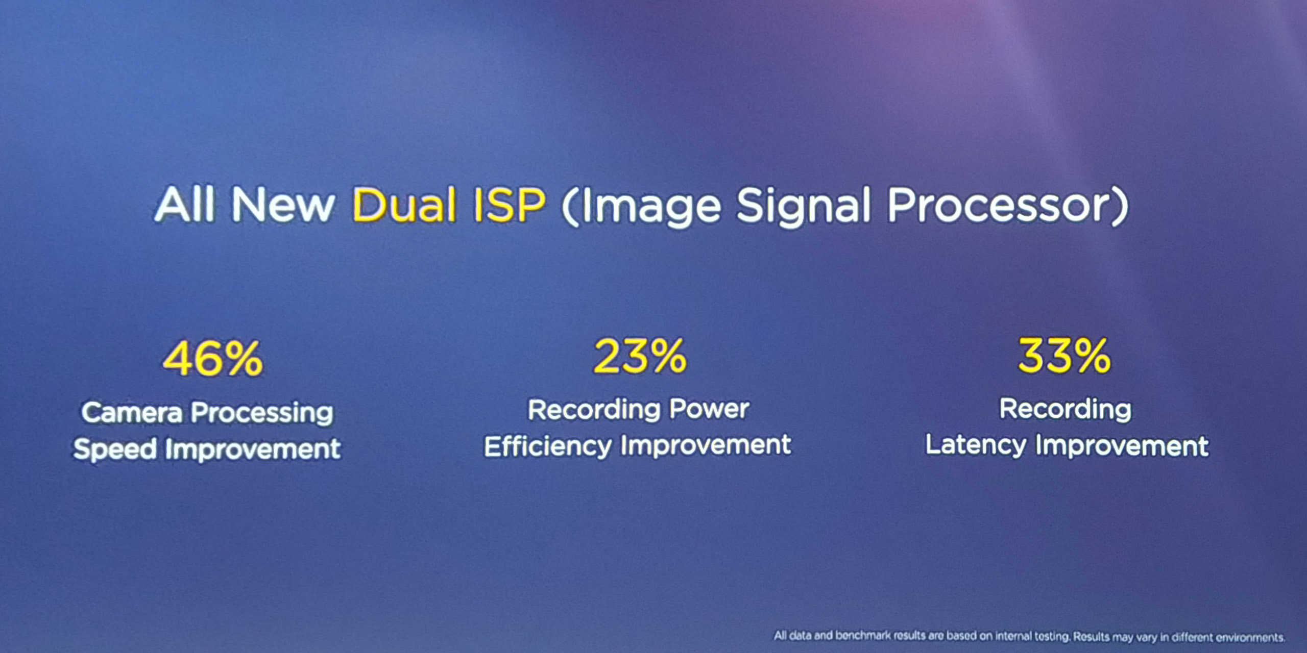
The new ISP is able to now use “multi-pass noise reduction”, which sound much like the multi-frame noise reduction features introduced in the Snapdragon 845 this year, where noise reduction is not perform on a spatial pixel basis, but on a temporal inter-frame basis, resulting in sharper noise-free images without the side-effect of blurring. There’s also a new video encoding pipeline which promises “33% shorter delay” between captures.
This last part was quite unclear in its meaning – the Kirin 970 lacked 4K60 encoding capabilities, and whether the Kirin supports it is something we still need to clarify with the company.
Update: We've confirmed with HiSilicon that the video encoder is still 4K30, which is a competitive disadvantage for the new SoC as it's not able to hold up to the competition's faster encoding capabilities.
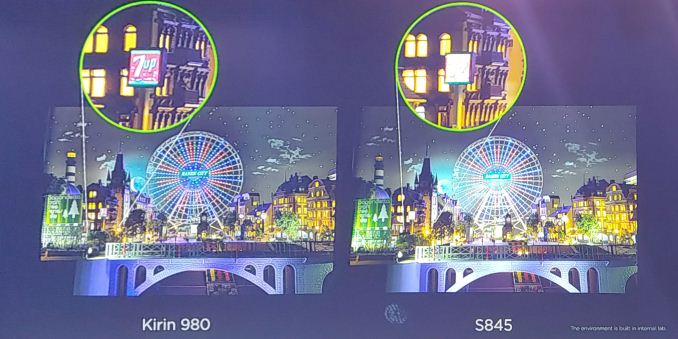
During the keynote presentation Huawei showcased the image quality advantage the Kirin 980 ISP had – in this scenario both test devices were using the same camera module with the same sensor, with the only difference being the HDR processing that differs.
New “Dual-NPU” at 2x the throughput
The Kirin 980 continues improving its neural network inference acceleration IP, and introduces a new “Dual NPU”. In fact what this means is that the block essentially has been doubled up in the same way you would add a scaling unit to a GPU. The block still only handles one model kernel at a time, meaning in effect the speed of a single inference should be doubled, depending on NN model of course.
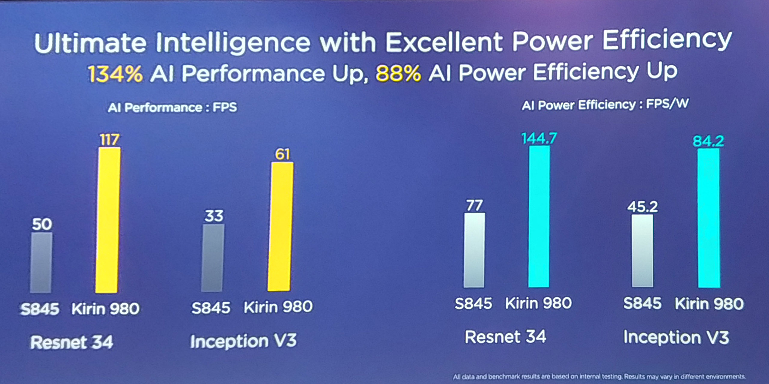
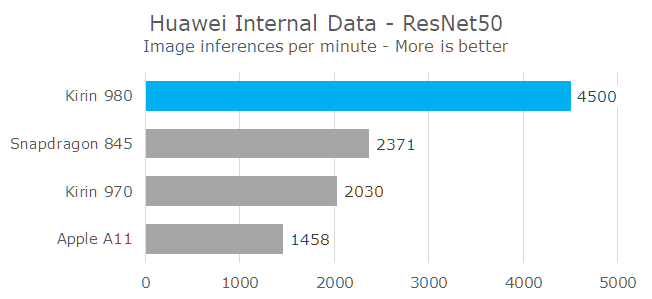
The new unit is said to be ~2.2x faster than the Kirin 970’s NPU, achieving up to 4500 inferences per minute, or 75 fps in their in-house test. They present figures for the Snapdragon 845 and Apple A11 as well, and as far as I can tell based on my own testing, these are very much accurate in terms of the observed performance.
Faster Category 21 integrated modem up to 1400Mbps + Balong 5000 5G Modem
The new modem in the Kirin 980 elevates the capabilities of the predecessor – now it’s able to support up to UE Cat 21 download speeds of up to 1400Mpbs. This is achieved of up to 3x carrier aggregation in combination of 4x4 MIMO, all while support 2x2 MIMO and new 256-QAM in the upload link (Category 18), and achieving 200Mbps upload speeds.
Alongside the Kirin 980 SoC, HiSilicon talked about its new 5G Balong 5000 modem. This is meant to be an accompanying chipset to the new Kirin 980 much in the same way the X50 is meant to be bundled with the next Snapdragon SoC. Unfortunately Huawei was light on details here, only proclaiming that we’ll see devices with the chipset combination sometime next year.
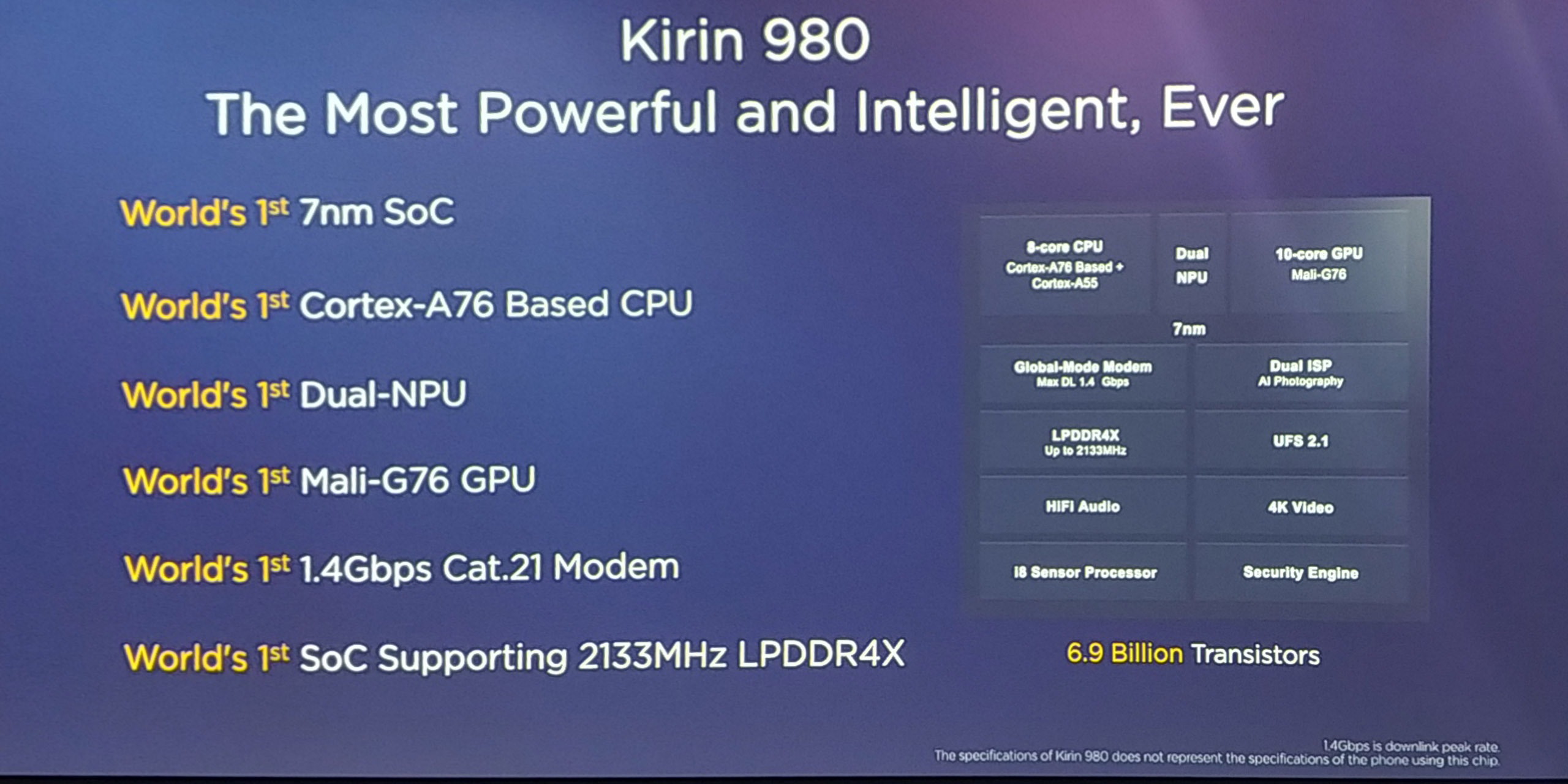
6.9bn transistors on <100mm² thanks to TSMC’s new 7nm manufacturing node
The new chipset boasts 6.9bn transistors – an increase of 25% compared to last year’s Kirin 970 coming in at 5.5bn. HiSilicon was able to maintain a small die area of less than 100mm² thanks to the new 7nm TSMC process node.

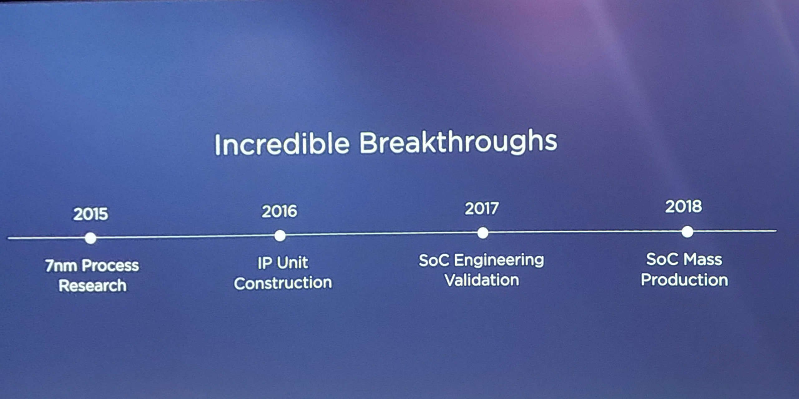
The project started in 2015 with 7nm process node research, with IP block unit development starting in 2016 and validation happening in 2017. Finally the SoC has been in mass production since this summer.
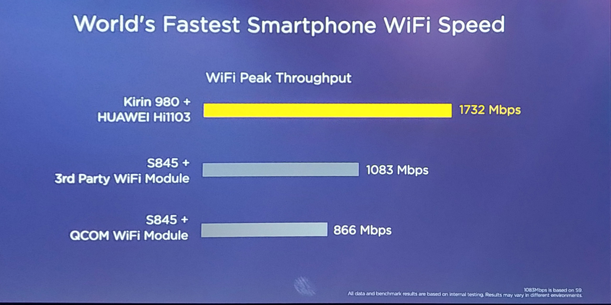
In-house WiFi Chipset
As surprise side-announcement was the reveal of the new Hi1103 WiFi chipset. The new chip supports 802.11ac with up to 1732Mbps speeds and 2x2 MIMO of up to 160MHz wide channels. I say that this is surprising because usually Huawei fell back to Broadcom BCM WiFi solutions which are considered to be industry leading and essentially found in every flagship device on the market. It’ll be interesting to see how the new HiSilicon chipset performs in comparison.
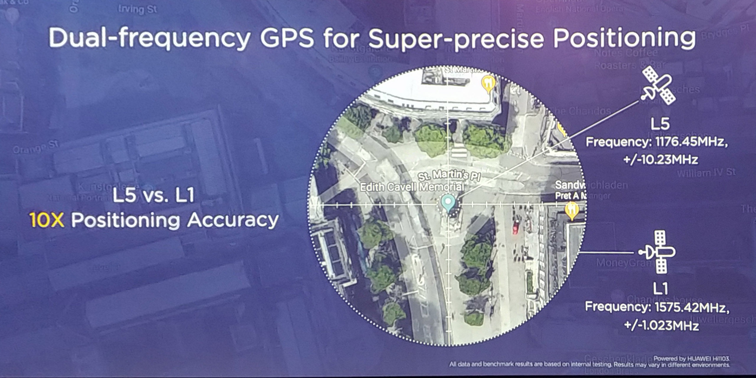
The new chipset also supports dual-frequency GPS with L5 frequencies – allowing up to 10x better position accuracy.
All the planets seem aligned for the Kirin 980
The Kirin 980 really does look like it’s on its way to be an exceptionally well balanced SoC with major improvements in every regard. The Kirin 960 and 970 had a rough time competing, both due to a process node disadvantage and then an IP disadvantage. Both suffered a lot from bad GPU performance and efficiency.
Here the Kirin 980 looks to resolve these issues and the combination of Arm’s new Cortex A76 CPU cores, G76 GPU, new internal IP blocks such as memory controller, ISP and updated NPU, combined with a new leading-edge 7nm manufacturing process. The combination of all these new characteristics put the new Kirin 980 in an excellent competitive position, and the upcoming Mate 20 is scheduled to be launch on October 16th, and should be a device to look forward to.


120 Comments
View All Comments
Ian Cutress - Friday, August 31, 2018 - link
Says right there in the articleSydneyBlue120d - Friday, August 31, 2018 - link
In the article and image only GPS is shown, and the Kirin 970 didn't support Galileo AFAIK :)Correct me if I'm wrong.
levizx - Friday, August 31, 2018 - link
You're wrong.SydneyBlue120d - Saturday, September 1, 2018 - link
Ok, can you share a screenshot of GPS test beta showing Galileo is being used with a Kyrin 970 then?Thanks a lot!
negusp - Sunday, September 2, 2018 - link
You're a dense idiot. Read the article.psychobriggsy - Monday, September 3, 2018 - link
Very rude to a reasonable question, especially when the article doesn't mention Galileo support. It only mentions L1 and L5 support from the GPS satellites.Still, L5 is welcome.
shabby - Friday, August 31, 2018 - link
Finally more then 30gb/sec of bandwidth, seems we were stuck at 30 for eons.jjj - Friday, August 31, 2018 - link
Sounds like scheduling will make or break this one.Their own WiFi solution adds a risk too- ofc best case scenario, it would be an upside.
Does it support uMCP memory solutions?
Dr. Swag - Friday, August 31, 2018 - link
Looks like TSMC 7nm density is looking good... Similar transistor count to GP104 for 1/3 the size. I can't wait to see what this means for 7nm amd and nvidia gpus.shabby - Friday, August 31, 2018 - link
This means Nvidia gpus will start at $999...