The NVIDIA Turing GPU Architecture Deep Dive: Prelude to GeForce RTX
by Nate Oh on September 14, 2018 12:30 PM ESTThe Turing Architecture: Volta in Spirit
Diving straight into the microarchitecture, the new Turing SM looks very different to the Pascal SM, but those who’ve been keeping track of Volta will notice a lot of similarities to the NVIDIA’s more recent microarchitecture. In fact, on a high-level, the Turing SM is fundamentally the same, with the notable exception of a new IP block: the RT Core. Putting the RT Cores and Tensor Cores aside for now, the most drastic changes from Pascal are same ones that differentiated Volta from Pascal. Turing’s advanced shading features are also in the same bucket in needing explicit developer support.
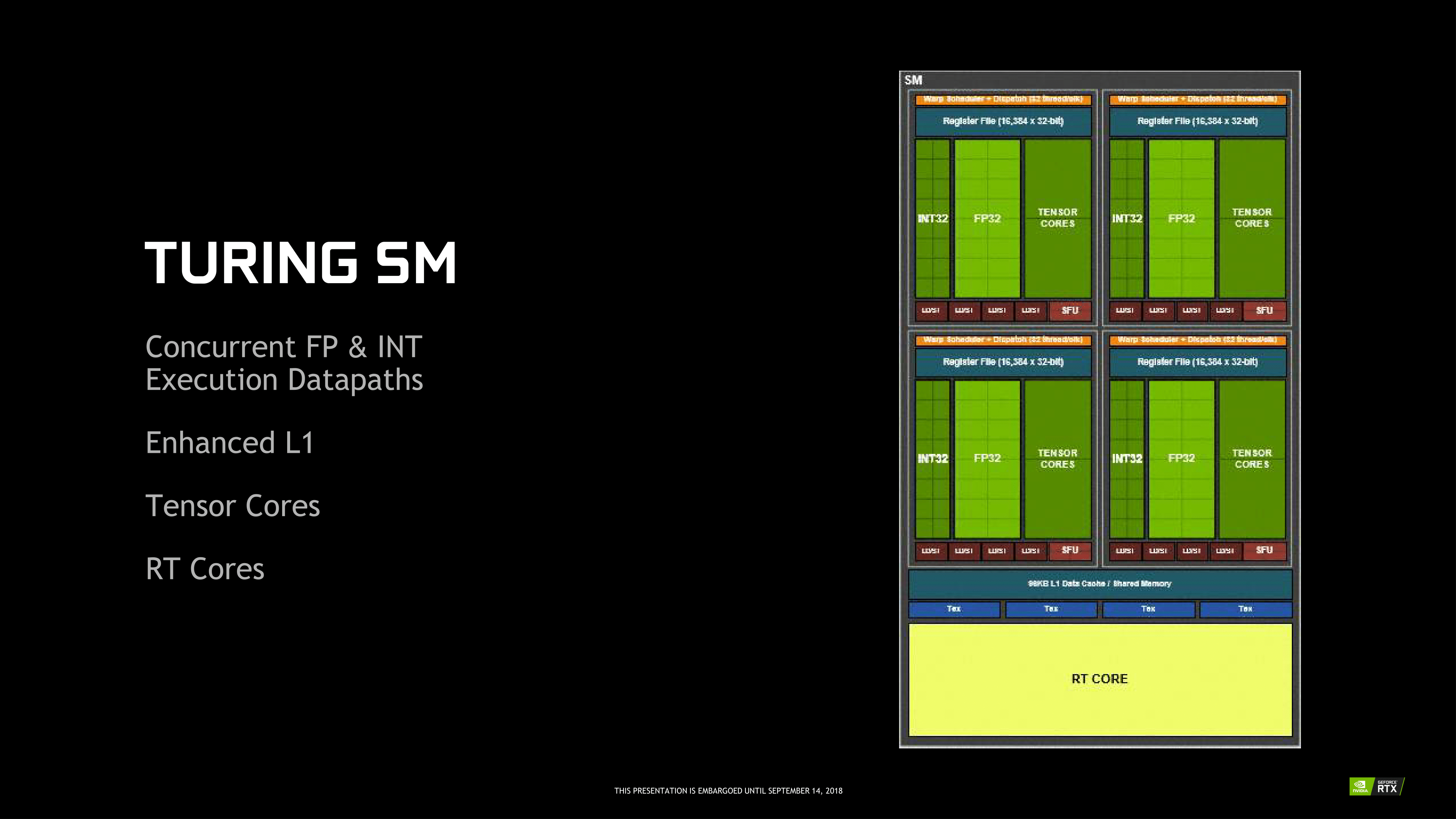
Like Volta, the Turing SM is partitioned into 4 sub-cores (or processing blocks) with each sub-core having a single warp scheduler and dispatch unit, as opposed Pascal’s 2 partition setup with two dispatch ports per sub-core warp scheduler. There are some fairly major implications with change, and broadly-speaking this means that Volta/Turing loses the capability to issue a second, non-dependent instruction from a thread for a single clock cycle. Turing is presumably identical to Volta performing instructions over two cycles but with schedulers that can issue an independent instruction every cycle, so ultimately Turing can maintain 2-way instruction level parallelism (ILP) this way, while still having twice the amount of schedulers over Pascal.
Like we saw in Volta, these changes go hand-in-hand with the new scheduling/execution model with independent thread scheduling that Turing also has, though differences were not disclosed at this time. Rather than per-warp like Pascal, Volta and Turing have per-thread scheduling resources, with a program counter and stack per-thread to track thread state, as well as a convergence optimizer to intelligently group active same-warp threads together into SIMT units. So all threads are equally concurrent, regardless of warp, and can yield and reconverge.

In terms of the CUDA cores and ALUs, the Turing sub-core has 16 INT32 cores, 16 FP32 cores, and 2 Tensor Cores, the same setup as the Volta sub-core. With the split INT/FP datapath model like Volta, Turing can also concurrently execute FP and INT instructions, which as we will see, is much more relevant with the RT cores involved. Where Turing differs is in lacking Volta’s full complement of FP64 cores, instead having a token amount (2 per SM) for compatibility reasons and resulting in FP64 throughput being 1/32 the TFLOP rate of FP32. Maimed FP64 is standard for NVIDIA’s consumer GPUs, but what has not been standard until now is Turing’s full 2x FP16 throughput, which was available in GP100 but was crippled in the other Pascal GPUs.
While these details may be more on the technical side of things, in Volta this design seemed inextricably linked to maximizing the most amount of performance from tensor cores, but minimizing disrupting parallelism or coordination with other compute workloads. The same is most likely true with Turing’s 2nd generation tensor cores and RT cores, where 4 independently scheduled sub-cores and granular thread manipulation would be very useful in extracting the most performance out of mixed gaming-oriented workloads, where rendering a single frame would be pulling in multiple blocks of the GPU to work in conjunction. This is actually a concept that circumscribes the RTX-OPS metric, and we will revisit that in depth later.
Memory-wise, every sub-core now has an L0 instruction cache like Volta, with identically sized 64 KB register file. In Volta, this was important in reducing latency when the tensor cores were in play, and in Turing this likely benefits RT cores similarly, which we will discuss in a later section. Otherwise, the Turing SM also has 4 load/store units per sub-core, down from 8 in Volta, but still maintains 4 texture units.
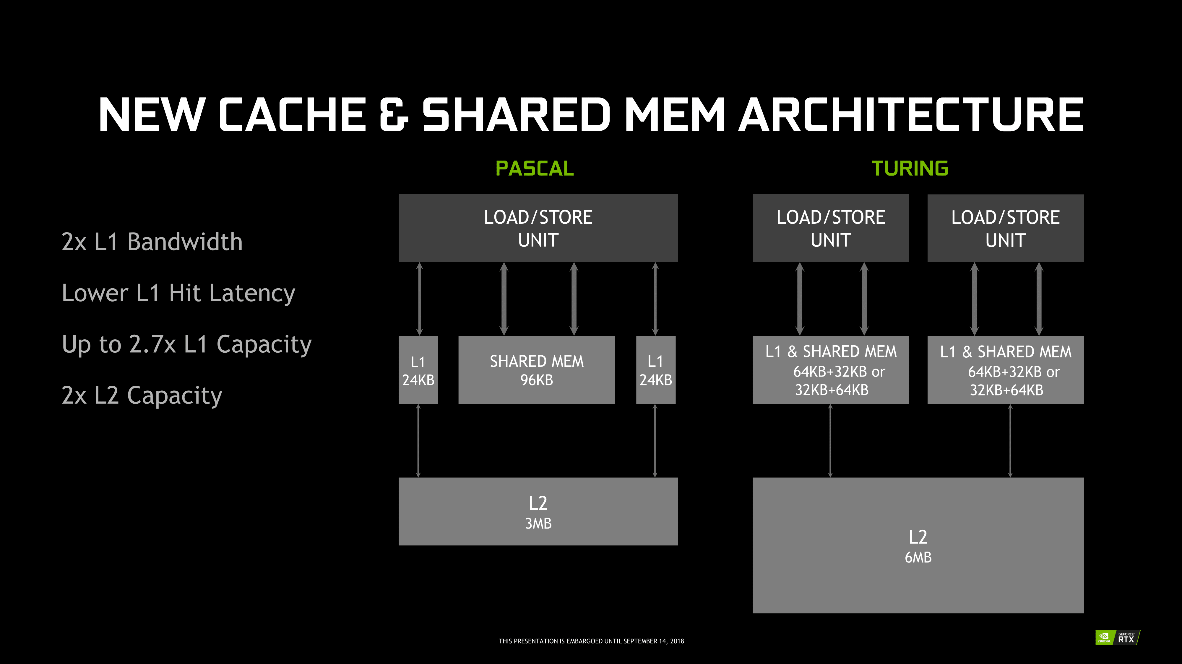
Further up the memory hierarchy is the new L1 data cache and Shared Memory (SMEM) that has been revamped and unified into a single partitionable memory block, another Volta innovation. For Turing, this is looking to be a combined 96 KB L1/SMEM, which traditional graphics workloads divide as 64KB for dedicated graphics shader RAM and as 32 KB for texture cache and register file spill area. Meanwhile, compute workloads can partition the L1/SMEM with up to 64 KB as L1 with the remaining 32 KB as SMEM, or vice versa. For Volta, SMEM can be configured up to 96 KB.
Though many of these details are only of value to developers, there are several important points to make here. One is simply how similar Turing and Volta are, as opposed to ; after all, they are in the same generational compute family. Another is how compute-oriented Volta – and by extension, Turing – are, and the fact that this is being brought to consumers as part of NVIDIA’s proclaimed ‘future of gaming.’ Part of that is, of course, permitting fast FP16 in potential gaming workloads, but Turing goes far beyond that. At the low level, Turing is less about maximizing traditional gaming, and more about maximizing gaming with special technologies such as real-time raytracing.
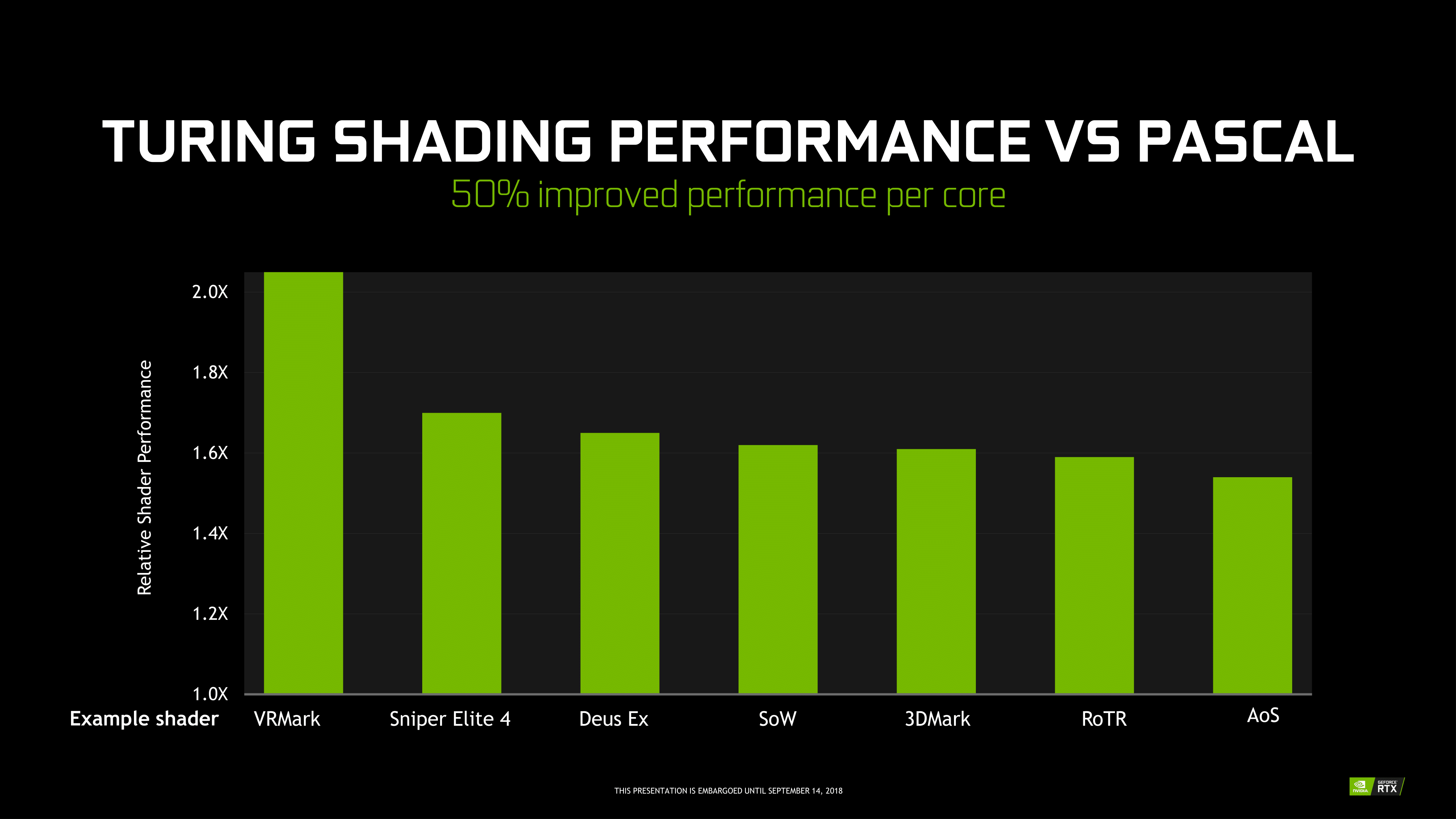
For their part, NVIDIA points to Turing’s leap in performance from Pascal, from memory hierarchy bandwidth uplifts to 50% more shader performance per core, but unfortunately for today we can’t connect this with any real world data or performance. With concurrent FP/INT execution in gaming, the company is keen to point out that around 36 INT instructions could be freed up by moving to its own pipe, which nevertheless doesn’t describe Turing performance, only the applicability of its concurrent execution feature in games.
It becomes a bit of a complex scenario, as we know that Volta already improved on Pascal in these aspects with concurrent execution, a brand new ISA, and reworked SM. And it doesn’t seem to involve architectural changes for significant clockspeed enhancements a la Pascal from Maxwell, though of course on the process side the 12nm FFN is a factor. So it comes down to special gaming workloads and real-world performance. The latter is not available today, but the former is so important to Turing that it merited dropping ‘GTX’ for ‘RTX’. And of those special workloads, real-time raytracing and RT cores take center stage.


111 Comments
View All Comments
gglaw - Saturday, September 15, 2018 - link
Why bother to make up statements claiming the prices are completely as expected with inflation added without even having a slight clue what the inflation rate has been in recent history? Outside of the very young readers here, most of us were around for 700 series, 8800, etc. and know first hand what type of changes inflation has had in the last 10-20 years. Especially comparing to the 980 Ti, and 1080 Ti, inflation has barely moved since those releases.Spunjji - Monday, September 17, 2018 - link
This. Most people here aren't stupid.notashill - Saturday, September 15, 2018 - link
700 series wasn't even close. 780 was $650->adjusted ~$700, 780Ti was $700->adjusted ~$760. And the 780 MSRP dropped to $500 after 6 months when the Ti launched.Santoval - Monday, September 17, 2018 - link
Yes, Navi will be midrange, at around a GTX 1080 performance level, or at best a bit faster. They initially planned a dual Navi package for the high end, linked by Infinity Fabric, but they canned (or postponed) it, due to the reluctance of game developers to support dual-die consumer graphics cards (according to AMD). They might release dual Navi professional graphics cards though.Tensor and RT cores should not be expected either. These will have to wait for the post-Navi (and post-GCN) generation.
TropicMike - Friday, September 14, 2018 - link
Good article. Lots of complicated stuff to try to explain.Just a quick typo on page 2: "It’s in pixel shaders that the various forms of lighting (shadows, reflection, reflection, etc) " I'm guessing you meant 'refraction' for one of those.
Smell This - Wednesday, July 3, 2019 - link
Super **Duper** Turbo Hyper Championship EditionYaldabaoth - Friday, September 14, 2018 - link
For the "eye diagram" on page 8, the texts says, "In this case we’re looking at a fairly clean eye diagram, illustrating the very tight 70ns transitions between data transfers." However, the image is labeled as "70 ps".Ryan Smith - Friday, September 14, 2018 - link
Nano. Pico. Really, it's a small difference... =PThanks!
Bulat Ziganshin - Friday, September 14, 2018 - link
It's not "Volta in spirit". It's Volta for the masses. The only differences- reduced FP64 cores
- reduced sharedmem/cache from 128 KB to 96 KB
- added RT cores
Now let's check what you want to change to produce "scientific" Turing GPU. Yes, exactly these things. So, despite the name, it's the same architecture, tuned for the gaming market
Yojimbo - Saturday, September 15, 2018 - link
You don't really know that. This article, as explained in the beginning, focuses only on the RT core improvements. There are other Turing features that were left out. I think we have no idea if Volta has variable rate shading, mesh shading,or multi-view rendering. I'm guessing it does not.Besides, what you said isn't true even limiting the discussion to what was covered in this article. The Turing Tensor cores allow for a greater range of precisions.