GlobalFoundries Stops All 7nm Development: Opts To Focus on Specialized Processes
by Anton Shilov & Ian Cutress on August 27, 2018 4:01 PM EST- Posted in
- Semiconductors
- CPUs
- AMD
- GlobalFoundries
- 7nm
- 7LP
What’s Next for GlobalFoundries?
In lieu of pursuing a 7nm platform, GlobalFoundries will be embarking on a multifaceted strategy for revenue and profitability. This strategy includes scaling out the 14LPP/12LP platform for various applications that are set to emerge in the 5G era, continuing to evolve the FD-SOI platform, spinning off its ASIC development business, further supporting its existing clients with their 14LPP/12LP products, and some other things.
Scaling Out the 14LPP/12LP
Originally designed for mobile SoCs and some other chips in mind, GlobalFoundries' 14LPP manufacturing technology is used to make CPUs and GPUs at GlobalFoundries. Furthermore, the company has designed two variations of this fabrication process. Whereas the base process used up to 13 metal layers and 9T libraries, 14HP was developed specifically for IBM and tailored for performance at the cost of transistor density, using up to 17 metal layers and 12T libraries. Meanwhile, 12LP — aimed at a broad spectrum of applications, including APUs/CPUs, automotive and other — uses 13 layers and 7.5T libraries, giving a 10% additional performance or power improvement as well as a 15% area reduction vs. the 14LPP.
Going forward, GlobalFoundries plans to offer a broader spectrum of technologies based on its 14 nm node. The move is not truly surprising. Samsung Foundry also offers three versions of its 14 nm processes: 14LPP for high-performance SoCs, 14LPC for compact SoCs, and 14LPU for ultra-low-power chips. So far, GlobalFoundries has confirmed three key markets of its future FinFET process technologies: RF, embedded memory, and low-power. In addition, the company plans to offer its 14LPP/12LP platform with enhanced performance and/or higher transistor density (for cost reduction). To do so, the company will be leveraging the knowledge and techniques they developed as part of the 7LP platform. But naturally Gary Patton does not want to disclose the nature of these innovations or any actual performance targets.
If the company succeeds in the integration of RF capabilities into FinFET-based chips, that will be a world’s first. In theory, such chips would have a notable edge over existing RF solutions, which are made using rather rough process technologies. In addition to regular RF capabilities, GlobalFoundries plans to offer features for mmWave radios. Embedded MRAM will also be another important feature of SoCs made using a FinFET fabrication tech as, again, nobody uses such transistors for embedded memory right now.
At the moment, GlobalFoundries is still forming its new development teams, so we do not know exactly how many projects the company will eventually work on. Meanwhile, keep in mind that any project started today will materialize at best in 2020, with actual products going into HVM in 2021. This will be in time for various devices for high-growth markets, but AMD will naturally wind down its 14LPP/12LP orders to GlobalFoundries over the 2019 – 2020 timeframe, reducing the company’s revenue and profits. Note that at present both the RF and embedded memory technologies for FinFET are in a pathfinding stage, so it is very hard to say when exactly GlobalFoundries comes up with appropriate process technologies.
Investing in FD-SOI
In addition to developing specialized versions of its FinFET-based process technologies, GlobalFoundries will continue to invest in its FDX-branded FD SOI-based platforms, such as 22FDX and 12FDX. Gary Patton did not pre-announce any new versions of the company’s FD-SOI fabrication processes, but clearly indicated that the FDX will remain very important for GlobalFoundries, which is not surprising as GF and Samsung Foundry are the only foundries to offer this tech.
Spinning Off ASICs
Designing chips for a new process technology is always a challenge both from engineering and financial points of view, especially for smaller companies. In a bid to help its customers to develop various SoCs, GlobalFoundries established its ASIC Solutions (ASICs) division, which helps the company’s customers in designing chips. Besides usual things like process development kits (PDKs), various design libraries, silicon-proven memory solutions, interfaces, and other necessary things, ASICs offers support from chip design, methodology, test and packaging teams.
Obviously, GlobalFoundries’ customers going forward will benefit from ASICs IP and teams. However, to ensure that the division continues to attract high-volume work, GlobalFoundries will spin it off and enable it to work with process technologies from other contract makers of semiconductors.
The Fate of EUV Tools
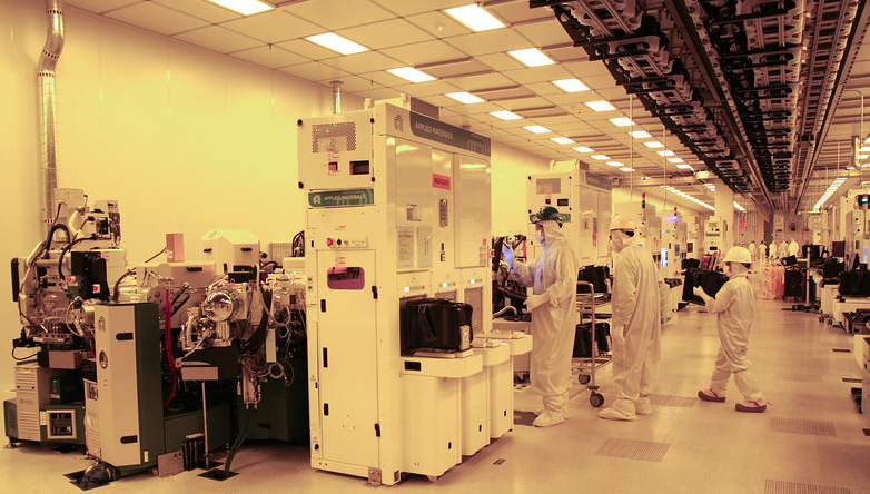
One of the questions we asked GlobalFoundries during a briefing concerning its strategic shift was about the fate of two ASML Twinscan NXE machines installed in Fab 8. At this point the company has not made any decisions, but it intends to consult with ASML and find out what would be the best use of these tools. In theory, GlobalFoundries could keep them to speed up prototyping or even production, but since they require a special treatment, keeping them without using them extensively for HVM may not be a good idea.
Some Thoughts
Until today, GlobalFoundries, Samsung Foundry, and TSMC were the only three remaining contract makers of semiconductors to offer leading-edge process technologies for logic. With GF dropping out from the race, Samsung and TSMC will be the only contract foundries remaining. (While Intel technically has foundry operations, they've had minimal impact on the industry).
For GlobalFoundries, the move has pros and cons. On the one hand the lion’s share of semiconductor industry revenue will be earned from chips made using ’12 nm’ and larger nodes even in 2022, according to Gartner’s findings and cited by GlobalFoundries. Evidently, by not competing for the leading edge, GF will reduce its R&D costs and necessity to build ultra-expensive EUV fabs for 2020 and onwards. Moreover, with specialized technologies sometimes tailored for particular clients, the company will better avoid directly competing against Samsung and TSMC in certain cases. Nonetheless, said foundries are going to compete for emerging devices as well, so they are going to design their own specialized fabrication processes (Samsung in particular will need them for itself). Therefore, GlobalFoundries is not exactly jumping into a blue ocean here.
What remains to be seen is how well GlobalFoundries manages to execute on the timely development of multiple new manufacturing processes and land new customers to fill Fab 8. The company will keep working with AMD for many years to come in fabbing current-generation CPUs and GPUs, and then switching exclusively to wafers with embedded APUs/GPUs as well as with first-gen EPYC dies, as these products have very long lifecycles. However, the number of wafers GlobalFoundries processes for AMD will be dropping rapidly starting from 2019. Whether GF will be able to substitute AMD’s orders with orders from enough smaller players to Fab 8 full utilized is something only time will tell.
While it is sad to see GlobalFoundries leaving the ‘bleeding edge’ field, it is evident that the company’s odds against Samsung and TSMC were not high enough for the owner and the management to take the risks. Therefore, it looks like ‘scaling out’ by offering a set of specialized (and maybe even unique) process technologies instead of ‘scaling up’ and offer another ‘bleeding edge’ node might just be a better bet for GlobalFoundries.
Related Reading:
- Change of Strategy: A New GlobalFoundries CEO in Dr. Thomas Caulfield
- The Future of Silicon: An Exclusive Interview with Dr. Gary Patton, CTO of GlobalFoundries
- GlobalFoundries Announces 22FDX Milestone: $2 Billion in Design Wins
- GlobalFoundries Gives 7 nm Capacity Update, Mulls Skipping 5 nm
- GlobalFoundries Weds FinFET and SOI in 14HP Process Tech for IBM z14 CPUs
- GlobalFoundries Adds 12LP Process for Mainstream and Automotive Chips; AMD Planning 12LP CPUs & GPUs
- GlobalFoundries Details 7 nm Plans: Three Generations, 700 mm², HVM in 2018
- GlobalFoundries to Expand Capacities, Build a Fab in China


127 Comments
View All Comments
RSAUser - Tuesday, August 28, 2018 - link
Their 7nm is probably slightly better than Intel 10nm.Think someone linked some papers a while back stating that TSMC and Samsung have likely already overtaken or are soon to overtake Intel.
eastcoast_pete - Tuesday, August 28, 2018 - link
I actually agree with the notion that x nm doesn't equal x nm when comparing different processes. However, Intel's 10 nm process has (continues to have?) had many teething problems, and scale-up has been delayed and apparently almost painful. My thought was that this is a potential chance for Intel to buy valuable IP, expertise and basically new state-of-the-art equipment at bargain basement prices. I know that they like to do everything as much in-house as possible, but Intel has made large acquisitions in recent years if they thought they would add to their bottom line.Kevin G - Monday, August 27, 2018 - link
1) Is the most likely scenario. Everyone is having problems as EUV is late for everyone and the alternatives are quad patterning which adds costs and slows production. It is a bag of hurt. 5 nm was looking like it could only be developed by masochists.2) Not improbable was GF was never that aggressive with their roadmap. The problem is that the other players hit delays so the reality likely was that GF was never going to be that far behind. Perception is everything. Spinning off 7 nm production would still require customers to come forward. This is a clear chicken and the egg scenario where the customers decided to roost else where.
As for other players purchasing GF, it is unlikely as companies like Intel actually have an excess of capacity for logic right now (DRAM and flash are slightly different which are higher utilized). The exception as noted would be keeping the US fabs in the Trusted Foundry Program. Certain stipulations had to be adhered to for GF to inherent those as part of the purchase of IBM's fabs. As such, there are likely conditions that still exist for the sale of those fabs. If another member of the Trusted Foundry Program just wanted those fabs, it would be far easier to change ownership.
bourbon_high - Monday, August 27, 2018 - link
Rumours last year said that the previous CEO Mr. Sanjay Jha and his team wanted to stop investing in 7 because the IBM led management team in Malta was behind and struggling. the current management team it seems was against 22fdx but pushed for 7nm. now after failing to deliver, the same management team under pressure from their investors and AMD have given up and seems to be calling it a strategy shift. Billions more wasted is what is said. GF needs new management, not dead weight IBM'ers that are slow to move if at all.rahvin - Monday, August 27, 2018 - link
The article clearly paints it as your number 2 scenario. When they did the math on buildout and customers they realized they'd loose money so they bagged the whole thing and decided to focus on their current process.Keep in mind there is still a ton of stuff fabbed on older process nodes, it can in fact by quite lucrative. With AMD unbound on manufacturing it also free's GloFo from having to spend billions building and upgrading Fabs. Given the rising costs in fabrication as they move up each node the market is likely to consolidate further and we could even see TSMC or Samsung drop out of the race due to the costs. Fab prices have gotten to the point of breaking budgets for even huge companies, there are very few companies that can afford to build a $20 billion EUV fab.
levizx - Tuesday, August 28, 2018 - link
You can't "spin-off" a process with NO FAB to produce it.eastcoast_pete - Tuesday, August 28, 2018 - link
Actually, you can, if you have a fab or two that can house the equipment and the people (the expertise) who are now being "made redundant" as the the British say. Processes have been moved ("migrated") from one fab to another in the past, although it can be a major pain in the derriere to do so.FullmetalTitan - Thursday, August 30, 2018 - link
Bigger issue then would be cost. Fab tool-in is expensive, even with retrofit work.Kevin G - Monday, August 27, 2018 - link
I wonder how this plays out for the Trusted Foundry programs that GF inherited from IBM. They allegedly had several contracts open with three letter agencies for specialized parts. Outside of that, they still provide some radiation hardened nodes as well (though far from state of the art). I'm not sure how profitable, if at all, things would be catering to those types of customers. While not high in volume, those due produce a nice margin. While the number bleeding edge nodes within the Trusted Foundry program is slim, there are plenty of players able to fab using older nodes. As the rest of the industry marches toward 7 nm and beyond, those other small time fabs will catch up.While IBM's contract with GF runs out at the end of this year, GF did develop a 12 nm FD-SOI process that looked like it was being used for a POWER9+ revision. Still those products would have been initially planned for a late 2019 release date.
btmedic04 - Monday, August 27, 2018 - link
My question in all of this is how will the fallout of Glofo abandoning 7nm affect AMD's 2nd gen Ryzen/Epyc processors