Hot Chips 2018: Samsung’s Exynos-M3 CPU Architecture Deep Dive
by Andrei Frumusanu on August 20, 2018 1:00 PM ESTThe Middle-Machine: Wider Decode, Rename, & Dispatch

Moving onto the middle machine (decoder, rename, dispatch), we come back to the fact that we see a 1.5x wider decode unit. Samsung isn’t disclosing any details here, but it has improved the instruction/µOP fusion capabilities. Rename and dispatch throughput match the decode width; here it’s important to not try to read too much into it and compare it to Arm’s CPU cores as we’re talking about different µOP types between the vendors. Here Samsung µarch has supported forms of multi-dispatch since the M1; the decoder emits a µOP which can dispatched to multiple schedulers simultaneously, but it still only counts it as one dispatch and one entry in the ROB.
In the integer core we see two additional schedulers, so the M3 is now able to issue 9 µOps over the 7 in the prior generations. One of the new ports is an additional ALU unit with multiplication capability, doubling the MUL throughput and increasing the simple integer arithmetic throughput by 25%.
The secondary additional port is a second load AGU which enables doubling of the load bandwidth of the core.
A "Beast" of a Floating Point Unit
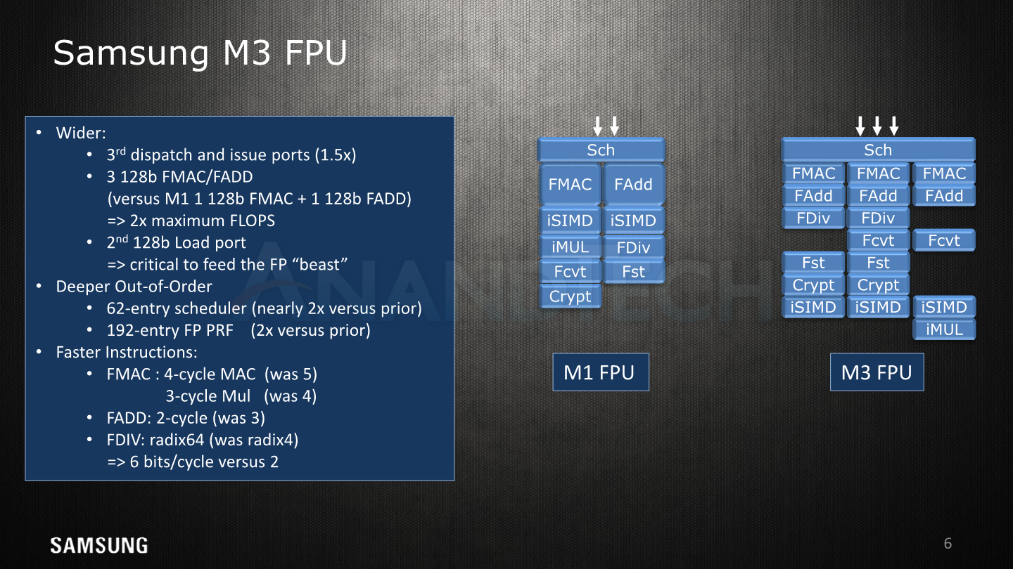
In the floating point core, we see a very different “beast” compared to the prior µarch. Here Samsung added a third pipeline, increasing the µOPs dispatched into and issued in the FPU. In terms of simple floating point capability, the M3 triples the multiply and arithmetic throughput by having 3 128b FMAC/FADD units over the M1’s single FMAC+FADD unit. In terms of FLOPS this represents a doubling of maximum throughput from 3 FLOPS (1x FMAC (2) + 1x FADD (1)) to 6 FLOPS (3x FMAC (2)).
Naturally because the execution throughput has increased so drastically it was necessary to scale up the scheduler and physical register files, doubling both of them from 32 to 62 for the schedulers and 96 to 192 entries for the FP PRFs.
Samsung has worked hard to reduce the execution latencies, and this also applies to the floating point pipelines. Here the multiplication unit has shaved off a cycle from 4 to 3 cycles also benefitting FMAC operations, going down from 5 to 4 cycles. Simple floating point addition shaved off a cycle from 3 to 2, as well as the FDIV seeing an upgrade to a Radix-64 unit significantly reducing division latencies.
Going on a little tangent here, I remember Arm had hyped its new floating point pipelines in the A76 for several years now, and they were very proud in the “state-of-the-art” VX datapaths of the new core. Well, at least from the higher level specifications it seems that Samsung beat Arm to the punch by a year as the M3 features equivalent floating point latencies while having higher execution throughput as well as even lower latency ASIMD capabilities. Obviously we’ll get to compare these in more detail in the future when we can test the silicon side-by-side.
New Load/Store Unit For Feeding It Data
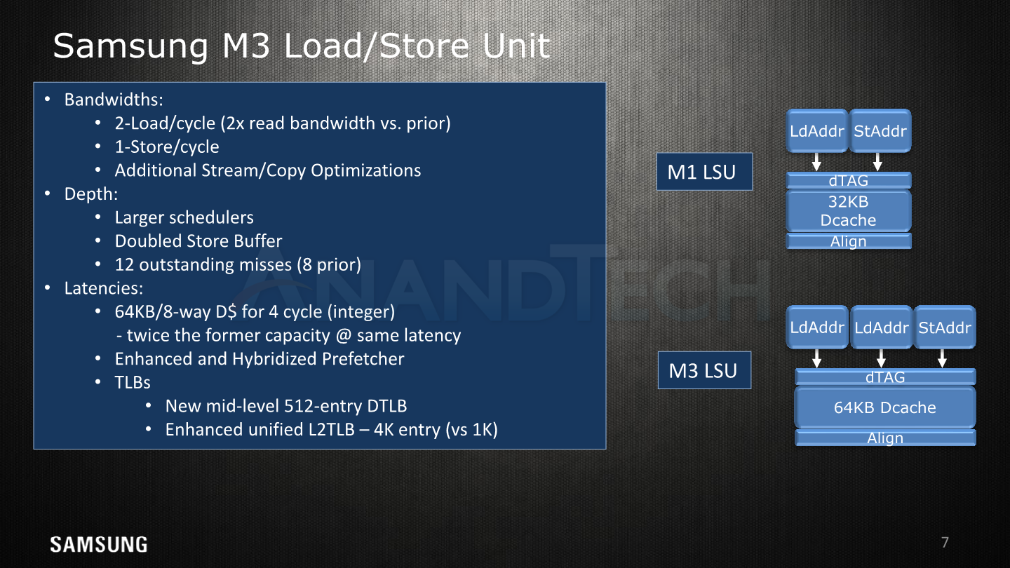
In the load/store unit we again see the doubling of the read bandwidth thanks to the addition of a second 128b load port. Here the load-use latency remains the same at 4-cycles. Store bandwidth is the same at 1 store per cycle with a 1-cycle latency. Again the M3 for this generation has a double bandwidth advantage as its two LD units operate at 128b/cycle versus 64b/cycle for the A75; the A76 will even this out next generation.
Overall the LD/ST scheduler’s capacities have been increased, and we see a doubling of the store buffer, although we don’t have exact values. To better serve the wider µarch, the outstanding misses on the L1 data cache has been increased from 8 to 12, meaning the unit can serve up to 12 concurrent data requests during cache misses while the core/system fetches the data from the higher-hierarchy cache levels or memory. This seems maybe low given the machine width of the M3 µarch – Arm hadn’t publicly disclosed the specifications for the A75 and prior in this regard but they made a MLP/memory level parallelism a big focus-point of the A76 disclosure, here the L1D services up to 20 outstanding misses which is more than the M3 can do, even though it’s a narrower machine.
Here Samsung’s prefetchers would need to be of top quality to avoid any memory bottlenecks and achieve the goal of an optimal perfect cache-hit operation, and indeed they say that there’s been enhancements into the new “hybridized” prefetchers. Here hybridized essentially means there’s going to be more prefetchers, or a single prefetchers able to deal with different kind of memory patterns.
The slides again mentioned the new TLB hierarchy we described earlier on the instruction side. Here on the data side we see the same 32-entry micro-DTLB as on the M1, however there’s now a new mid-level DTLB with 512 entries. Both the instruction TLBs and data TLBs are now serviced by an enhanced and larger unified L2 TLB with 4096 entries versus the 1024 entries in the prior generation.
Core Pipeline: Everything Has A Cost
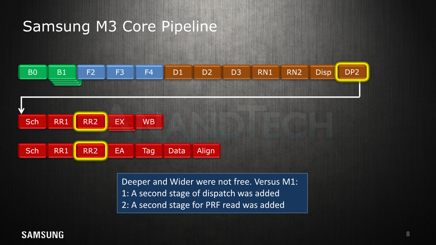
Naturally widening the microarchitecture comes at a cost, and the M3 adds two cycles to its pipeline depth when compared to the Exynos M1. A secondary dispatch stage was added, as well as a second stage for register read. Usually CPU pipeline depth is counted as the stages from predict/branch to register write-back, and in this case the M3 is quite deep at 17 stages, versus 15 stages for the M1 and 13 stages for the A75 and A76.
Branch misprediction penalty is 16 cycles as there’s a drive cycle back to the frontend, again 2 cycles more than the 14c penalty on the M1. Samsung didn’t say if the µarch had any kind of other fast-paths between the stages to reduce latencies in critical cases. The M3, and partly the M1’s disadvantages over its Arm counterpart are located in the 3 vs 2-stages fetch and decode units (+2 stages), a 2 vs 1-stage register rename unit (+1), and the need for a second dispatch stage (+1).
Samsung admits that while this is a negative, it was a necessary evil in order to get the bigger µarch done on schedule, and while the machine does well with branch mispredicts, it is a cost for the new µarch.
In general it’s odd to see that Samsung’s deeper microarchitecture choices haven’t actually resulted in much of a clock speed advantage in actual products. Here it seems that the competition might be doing a better job in the physical design and the limiting critical paths in order to achieve higher frequencies at reasonable voltages.
A New 3-Level Cache Hierarchy
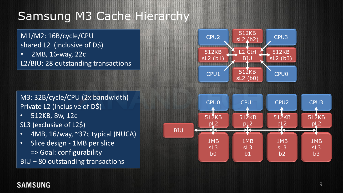
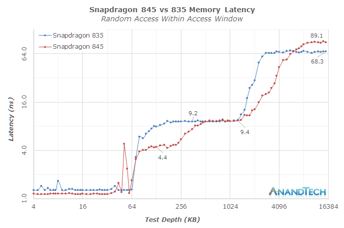
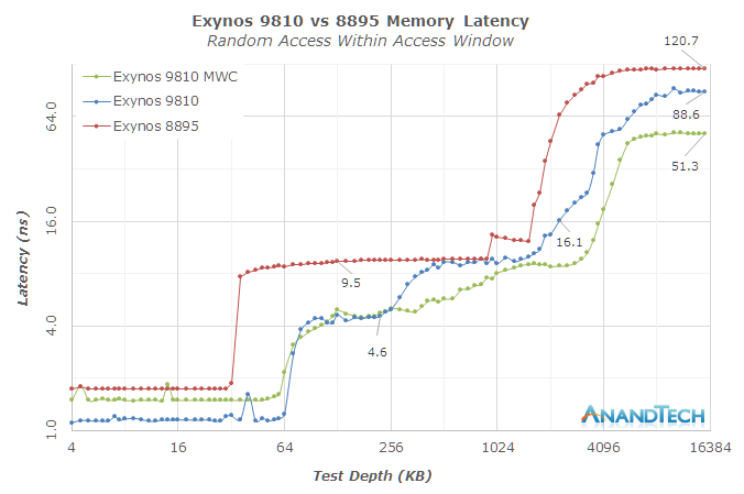
Moving away from the CPU core itself, we’re having a look at the new L2/L3 cache hierarchy. Like the A75 and A76, the M3 introduced a new private L2 cache as an intermediate level between the core and the shared last-level cache. The new private L2 is inclusive of the lower data caches and comes at 512KB per core. The access latency versus the shared L2 in the M1 was reduced from 22 cycles down to 12 cycles. Here it seems that Samsung would be at a disadvantage to Arm’s A75 as the latter discloses a L2 hit latency of only 8 cycles. It’s to be noted that in actual physically implemented silicon this figure might go up due to design choices in the RAMs and physical layout. In practice the Snapdragon 845’s L2 latencies at 2.8GHz measure in at ~4.4ns versus ~4.6ns for a 2.7GHz Exynos 9810 in our measurements.
Bandwidth to the L2 cache has also been doubled, now achieving 32B/cycle versus 16B/cycle for the M1. The A75 for comparison reads 16B/cycle from the L2 while writing into it at 32B/cycle.
At first there was a bit of a confusion when the Exynos 9810 was announced as to how its L3 cache works. Eventually we got clarification that Arm doesn’t actually allow third-party cores to plug into its DynamiQ cluster/L3 system, and the die shot of the new SoC finally undoubtedly confirmed that the new silicon has nothing to do with Arm’s counterpart.
Here we see a large 4MB cache implemented in a NUCA (Non-uniform cache architecture) fashion with four slices of 1MB, with each slice being located opposite of a CPU core. Because of the non-uniform layout, the access latencies between the cores and the slices are not the same. A core accessing an adjacent slice has latencies of 32 cycles, while the furthest distance between a CPU and slice has latencies of 44 cycles. Samsung quotes an average latency of 37 cycles in typical patterns.
It’s here where the M3 seems to be weaker compared to Arm’s implementation. Arm quoted L3 hit latencies of 25 cycles for an A75. In practice again we see the Snapdragon 845 achieving ~9.4ns while the Exynos 9810 starts at ~11ns nearest to the depth size of the L2 cache and goes up to ~20ns reaching the 4MB test depth of the L3. Here the fact that that Samsung’s L3 implementation is meant to be run at higher frequencies (2.7GHz in the above values) and is on the same clock plane as the CPUs doesn’t help it as the cycle access latency disadvantage is too great, even in the face of the lower clocked 1478MHz DSU of the Snapdragon 845. While the DSU’s lower maximum clock can be a disadvantage, it is actually very much an advantage in the opposite scenario; when the CPU cores are clocked lower, they could still take advantage of a fast running DSU/L3 cache and its lower latencies. The M3’s cache hierarchy in contrast slows down along with its CPU cores.
The M1/M2’s bus unit handled up to 28 outstanding misses while the M3’s handles up to 80 outstanding misses – there’s a lack clarity here on if this applies to the L3 or if somehow the L2 blocks are included in this figure. Arm never talked about the A75’s capabilities here but details that the A76 is be able to handle 46 outstanding misses on the L2 caches with 94 outstanding misses on the DSU’s L3.
Data partitioning between the L3 slices is decided by address hash, and all slices are powered on at the same time. In contrast, a DSU in a larger SoC is by default implemented with two slices, of each which can be half powered down – giving a granularity of ¼ of the L3 in terms of power-down capability. I’m not sure how the SD845 is implemented here as it’s difficult to determine it on a lower-resolution die shot.
Finally Samsung explains this slice design is meant to achieve better configurability for different designs beyond premium mobile, which of course is still the highest priority. Samsung is likely pointing at either large form-factor designs or what I may think is more likely, S.LSI’s efforts in the automotive space.
Overall for the cache hierarchy Samsung admits that the end product didn’t quite achieve what they really wanted. The end-product ended up like this because of necessary trade-off to make in order to get the 3-level cache hierarchy implemented for this generation. Here I think we’ll a much larger focus for the next generation M4.


45 Comments
View All Comments
Dunatis - Tuesday, August 21, 2018 - link
Was this article written by an English speaker or translated through google translate or something. Apart from the other bits, this is truly the worst sentence I have read in a long while: We’ve exclusively first reported on the details of the new microarchitecture back in January and it was clear from that point on that this was a big one: Samsung had went for a huge push in terms of performance, resulting in one of the biggest generational jumps of any silicon CPU designer in recent history.darkich - Tuesday, August 21, 2018 - link
I don't see a problem?Looks like you either have basic comprehension issues, or English language understanding issues.
sonofgodfrey - Tuesday, August 21, 2018 - link
So, I don't have the best grammar in the world, but I think this is better:We first reported on the details of the new microarchitecture exclusively back in January, and it was clear from that point on that this a big one. Samsung had gone for a huge performance push, resulting in one of the biggest generational jumps of any CPU design in recent history.
sonofgodfrey - Tuesday, August 21, 2018 - link
that this a big one - That should be: that this was a big one.name99 - Wednesday, August 22, 2018 - link
I suspect Andrei speaks rather better German or French than you do.You might still think you're living in the 1950s, but the rest of us are well aware that it's the 21st Century; and it's just basic good manners to be grateful that so many smart people in the world are willing to speak English, rather than complaining that they don't do so perfectly.
abufrejoval - Friday, August 24, 2018 - link
Probably need to add Romanian and Lëtzebuergesch.darkich - Tuesday, August 21, 2018 - link
"Here’s to hoping S.LSI and SARC resolve the Exynos 9810 and M3’s weaknesses"Can you please clarify in layman terms ..does this mean there is a chance that Note 9's Exynos could be ironed out compared to S9 one you tested?
Btw, have to admit the depth and thoroughness of your articles are pretty mind blowing.
Andrei Frumusanu - Tuesday, August 21, 2018 - link
No, it refers to fixing the inherent hardware limitations in the M4 next year.jimjamjamie - Tuesday, August 21, 2018 - link
"µarch width and µarch width are complementary to each other for performance"I mean I guess this isn't incorrect, but I don't think that's what you meant to say, Andrei :)
lilmoe - Tuesday, August 21, 2018 - link
The M3 should have just been an iterative improvement over the M2, as the M2 was over the M1. The M3 was rushed in design, execution and process node. So much untapped potential.Oh well... I guess the M3 was a good beta for optimizing the M4 further, while retaining its competitiveness with Qualcomm and Apple in real world usage. I have no doubt the M4 will be best in class, but I just can't hide the fact that the M3 left a bitter taste in my mouth; it should have been a clear win from all aspects.