Hot Chips 2018: Samsung’s Exynos-M3 CPU Architecture Deep Dive
by Andrei Frumusanu on August 20, 2018 1:00 PM ESTThe Middle-Machine: Wider Decode, Rename, & Dispatch

Moving onto the middle machine (decoder, rename, dispatch), we come back to the fact that we see a 1.5x wider decode unit. Samsung isn’t disclosing any details here, but it has improved the instruction/µOP fusion capabilities. Rename and dispatch throughput match the decode width; here it’s important to not try to read too much into it and compare it to Arm’s CPU cores as we’re talking about different µOP types between the vendors. Here Samsung µarch has supported forms of multi-dispatch since the M1; the decoder emits a µOP which can dispatched to multiple schedulers simultaneously, but it still only counts it as one dispatch and one entry in the ROB.
In the integer core we see two additional schedulers, so the M3 is now able to issue 9 µOps over the 7 in the prior generations. One of the new ports is an additional ALU unit with multiplication capability, doubling the MUL throughput and increasing the simple integer arithmetic throughput by 25%.
The secondary additional port is a second load AGU which enables doubling of the load bandwidth of the core.
A "Beast" of a Floating Point Unit
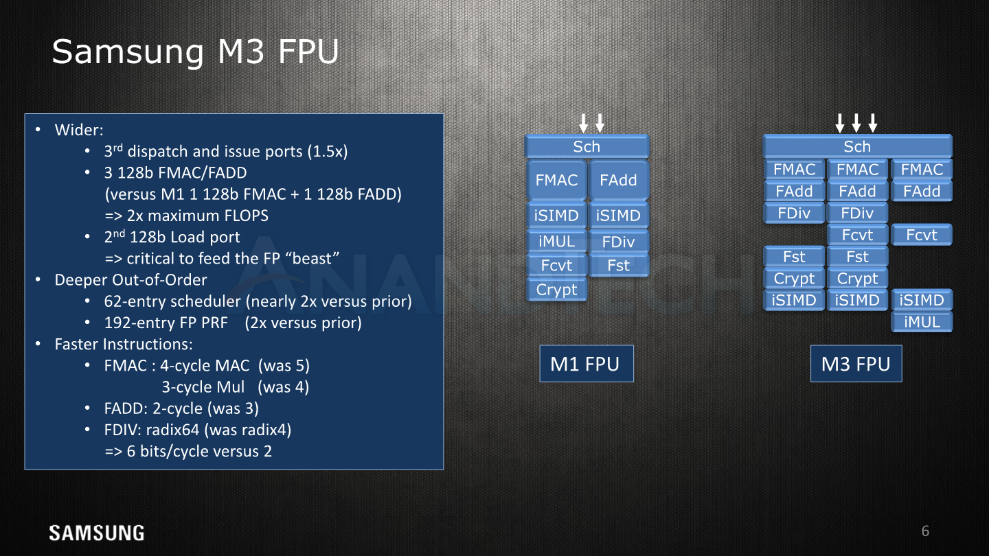
In the floating point core, we see a very different “beast” compared to the prior µarch. Here Samsung added a third pipeline, increasing the µOPs dispatched into and issued in the FPU. In terms of simple floating point capability, the M3 triples the multiply and arithmetic throughput by having 3 128b FMAC/FADD units over the M1’s single FMAC+FADD unit. In terms of FLOPS this represents a doubling of maximum throughput from 3 FLOPS (1x FMAC (2) + 1x FADD (1)) to 6 FLOPS (3x FMAC (2)).
Naturally because the execution throughput has increased so drastically it was necessary to scale up the scheduler and physical register files, doubling both of them from 32 to 62 for the schedulers and 96 to 192 entries for the FP PRFs.
Samsung has worked hard to reduce the execution latencies, and this also applies to the floating point pipelines. Here the multiplication unit has shaved off a cycle from 4 to 3 cycles also benefitting FMAC operations, going down from 5 to 4 cycles. Simple floating point addition shaved off a cycle from 3 to 2, as well as the FDIV seeing an upgrade to a Radix-64 unit significantly reducing division latencies.
Going on a little tangent here, I remember Arm had hyped its new floating point pipelines in the A76 for several years now, and they were very proud in the “state-of-the-art” VX datapaths of the new core. Well, at least from the higher level specifications it seems that Samsung beat Arm to the punch by a year as the M3 features equivalent floating point latencies while having higher execution throughput as well as even lower latency ASIMD capabilities. Obviously we’ll get to compare these in more detail in the future when we can test the silicon side-by-side.
New Load/Store Unit For Feeding It Data
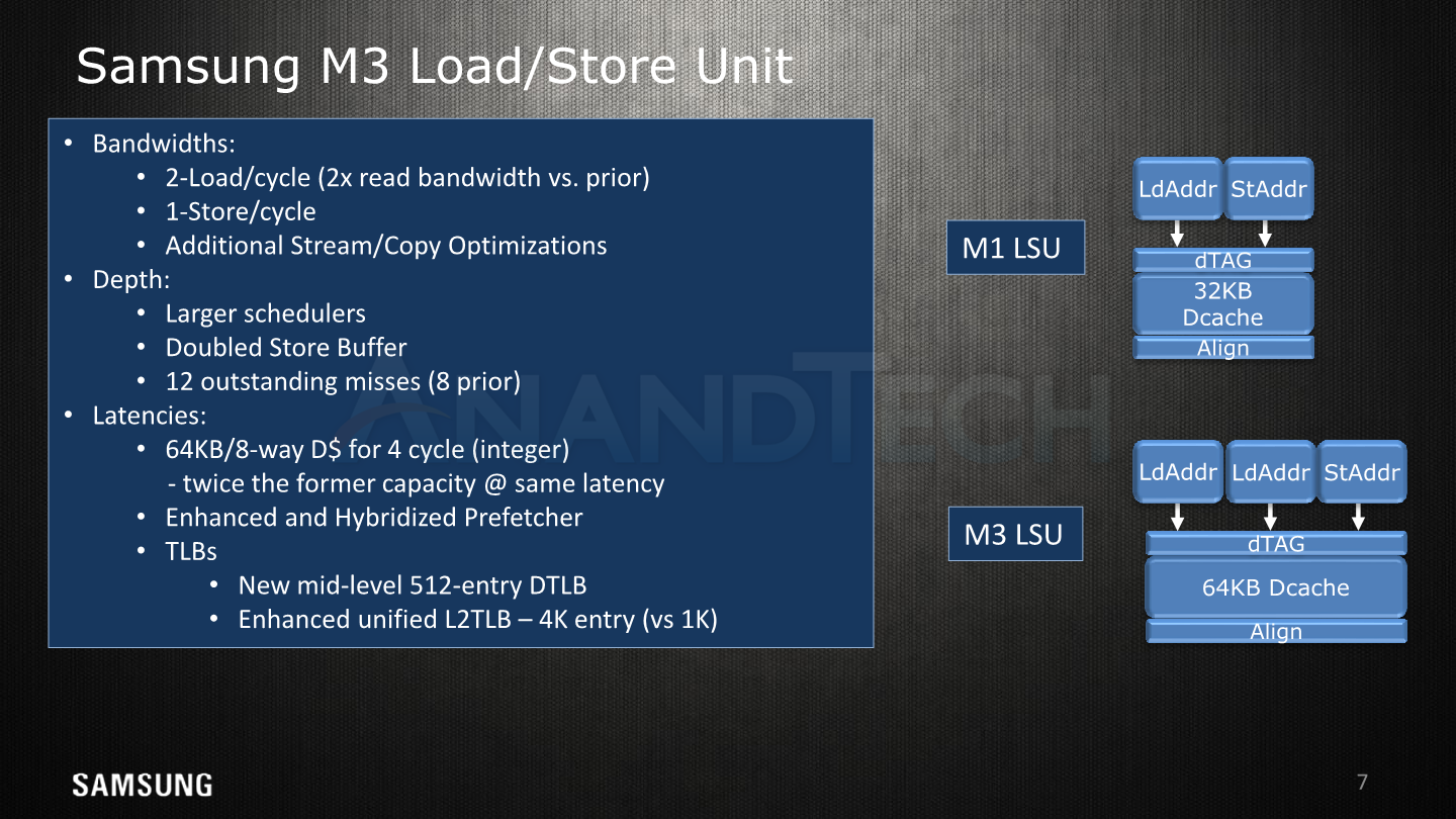
In the load/store unit we again see the doubling of the read bandwidth thanks to the addition of a second 128b load port. Here the load-use latency remains the same at 4-cycles. Store bandwidth is the same at 1 store per cycle with a 1-cycle latency. Again the M3 for this generation has a double bandwidth advantage as its two LD units operate at 128b/cycle versus 64b/cycle for the A75; the A76 will even this out next generation.
Overall the LD/ST scheduler’s capacities have been increased, and we see a doubling of the store buffer, although we don’t have exact values. To better serve the wider µarch, the outstanding misses on the L1 data cache has been increased from 8 to 12, meaning the unit can serve up to 12 concurrent data requests during cache misses while the core/system fetches the data from the higher-hierarchy cache levels or memory. This seems maybe low given the machine width of the M3 µarch – Arm hadn’t publicly disclosed the specifications for the A75 and prior in this regard but they made a MLP/memory level parallelism a big focus-point of the A76 disclosure, here the L1D services up to 20 outstanding misses which is more than the M3 can do, even though it’s a narrower machine.
Here Samsung’s prefetchers would need to be of top quality to avoid any memory bottlenecks and achieve the goal of an optimal perfect cache-hit operation, and indeed they say that there’s been enhancements into the new “hybridized” prefetchers. Here hybridized essentially means there’s going to be more prefetchers, or a single prefetchers able to deal with different kind of memory patterns.
The slides again mentioned the new TLB hierarchy we described earlier on the instruction side. Here on the data side we see the same 32-entry micro-DTLB as on the M1, however there’s now a new mid-level DTLB with 512 entries. Both the instruction TLBs and data TLBs are now serviced by an enhanced and larger unified L2 TLB with 4096 entries versus the 1024 entries in the prior generation.
Core Pipeline: Everything Has A Cost
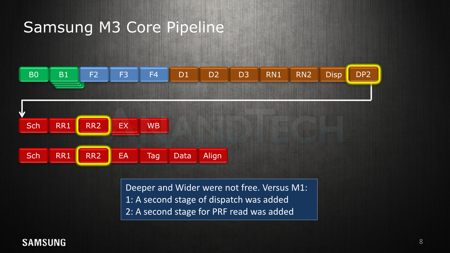
Naturally widening the microarchitecture comes at a cost, and the M3 adds two cycles to its pipeline depth when compared to the Exynos M1. A secondary dispatch stage was added, as well as a second stage for register read. Usually CPU pipeline depth is counted as the stages from predict/branch to register write-back, and in this case the M3 is quite deep at 17 stages, versus 15 stages for the M1 and 13 stages for the A75 and A76.
Branch misprediction penalty is 16 cycles as there’s a drive cycle back to the frontend, again 2 cycles more than the 14c penalty on the M1. Samsung didn’t say if the µarch had any kind of other fast-paths between the stages to reduce latencies in critical cases. The M3, and partly the M1’s disadvantages over its Arm counterpart are located in the 3 vs 2-stages fetch and decode units (+2 stages), a 2 vs 1-stage register rename unit (+1), and the need for a second dispatch stage (+1).
Samsung admits that while this is a negative, it was a necessary evil in order to get the bigger µarch done on schedule, and while the machine does well with branch mispredicts, it is a cost for the new µarch.
In general it’s odd to see that Samsung’s deeper microarchitecture choices haven’t actually resulted in much of a clock speed advantage in actual products. Here it seems that the competition might be doing a better job in the physical design and the limiting critical paths in order to achieve higher frequencies at reasonable voltages.
A New 3-Level Cache Hierarchy
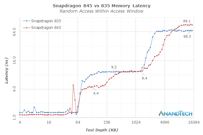
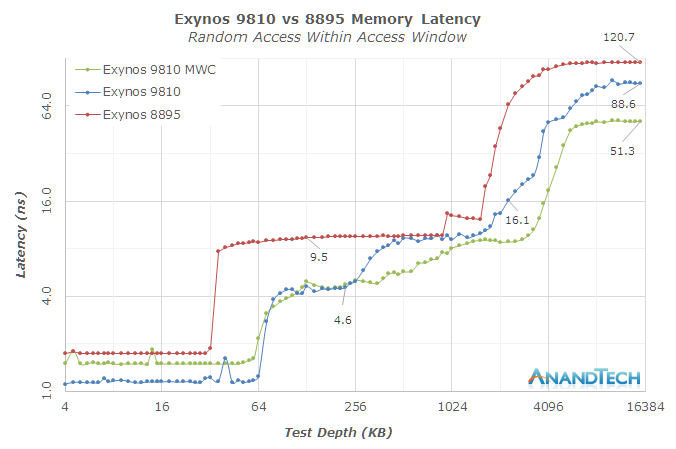
Moving away from the CPU core itself, we’re having a look at the new L2/L3 cache hierarchy. Like the A75 and A76, the M3 introduced a new private L2 cache as an intermediate level between the core and the shared last-level cache. The new private L2 is inclusive of the lower data caches and comes at 512KB per core. The access latency versus the shared L2 in the M1 was reduced from 22 cycles down to 12 cycles. Here it seems that Samsung would be at a disadvantage to Arm’s A75 as the latter discloses a L2 hit latency of only 8 cycles. It’s to be noted that in actual physically implemented silicon this figure might go up due to design choices in the RAMs and physical layout. In practice the Snapdragon 845’s L2 latencies at 2.8GHz measure in at ~4.4ns versus ~4.6ns for a 2.7GHz Exynos 9810 in our measurements.
Bandwidth to the L2 cache has also been doubled, now achieving 32B/cycle versus 16B/cycle for the M1. The A75 for comparison reads 16B/cycle from the L2 while writing into it at 32B/cycle.
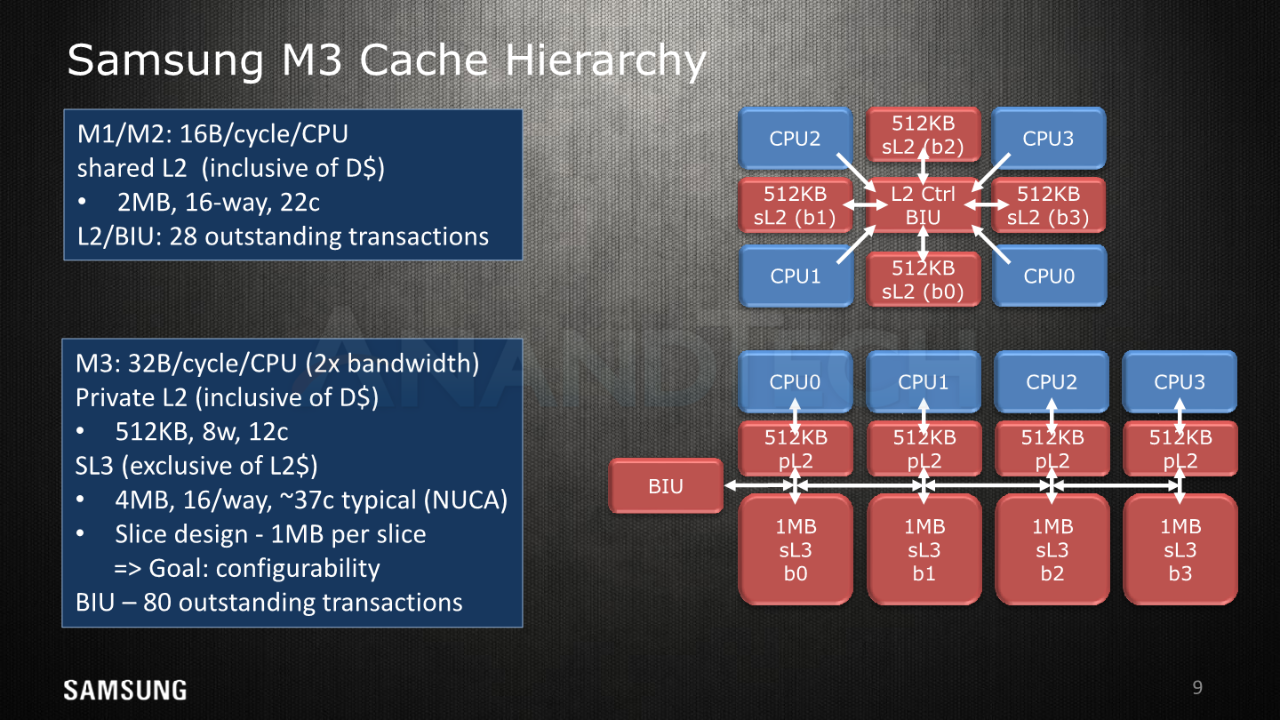
At first there was a bit of a confusion when the Exynos 9810 was announced as to how its L3 cache works. Eventually we got clarification that Arm doesn’t actually allow third-party cores to plug into its DynamiQ cluster/L3 system, and the die shot of the new SoC finally undoubtedly confirmed that the new silicon has nothing to do with Arm’s counterpart.
Here we see a large 4MB cache implemented in a NUCA (Non-uniform cache architecture) fashion with four slices of 1MB, with each slice being located opposite of a CPU core. Because of the non-uniform layout, the access latencies between the cores and the slices are not the same. A core accessing an adjacent slice has latencies of 32 cycles, while the furthest distance between a CPU and slice has latencies of 44 cycles. Samsung quotes an average latency of 37 cycles in typical patterns.
It’s here where the M3 seems to be weaker compared to Arm’s implementation. Arm quoted L3 hit latencies of 25 cycles for an A75. In practice again we see the Snapdragon 845 achieving ~9.4ns while the Exynos 9810 starts at ~11ns nearest to the depth size of the L2 cache and goes up to ~20ns reaching the 4MB test depth of the L3. Here the fact that that Samsung’s L3 implementation is meant to be run at higher frequencies (2.7GHz in the above values) and is on the same clock plane as the CPUs doesn’t help it as the cycle access latency disadvantage is too great, even in the face of the lower clocked 1478MHz DSU of the Snapdragon 845. While the DSU’s lower maximum clock can be a disadvantage, it is actually very much an advantage in the opposite scenario; when the CPU cores are clocked lower, they could still take advantage of a fast running DSU/L3 cache and its lower latencies. The M3’s cache hierarchy in contrast slows down along with its CPU cores.
The M1/M2’s bus unit handled up to 28 outstanding misses while the M3’s handles up to 80 outstanding misses – there’s a lack clarity here on if this applies to the L3 or if somehow the L2 blocks are included in this figure. Arm never talked about the A75’s capabilities here but details that the A76 is be able to handle 46 outstanding misses on the L2 caches with 94 outstanding misses on the DSU’s L3.
Data partitioning between the L3 slices is decided by address hash, and all slices are powered on at the same time. In contrast, a DSU in a larger SoC is by default implemented with two slices, of each which can be half powered down – giving a granularity of ¼ of the L3 in terms of power-down capability. I’m not sure how the SD845 is implemented here as it’s difficult to determine it on a lower-resolution die shot.
Finally Samsung explains this slice design is meant to achieve better configurability for different designs beyond premium mobile, which of course is still the highest priority. Samsung is likely pointing at either large form-factor designs or what I may think is more likely, S.LSI’s efforts in the automotive space.
Overall for the cache hierarchy Samsung admits that the end product didn’t quite achieve what they really wanted. The end-product ended up like this because of necessary trade-off to make in order to get the 3-level cache hierarchy implemented for this generation. Here I think we’ll a much larger focus for the next generation M4.


45 Comments
View All Comments
name99 - Wednesday, August 22, 2018 - link
The issue is not technology (everyone knows CDMA basics because you need it on the data side for WCDMA aka 3G). The issue is licensing.Maybe QC changes the licensing terms so that doing it in-house was simply not worth the cost? This seems very much in-line with the world-wide lawsuits against QC for various anti-competitive behavior.
petar_b - Saturday, November 3, 2018 - link
I when they use Exynos they have less royalty fees to pay since it's their own processor. EU market is smaller than the US or ASIA so they compensate by providing chip with cheaper costs.PS - CDMA, modem and all other reasons mentioned are irrelevant; other brands use Qualcom in EU and all works perfectly.
AlB80 - Monday, August 20, 2018 - link
Unused cores do not consume energy at all regardless of voltage. Thus there should be two threads on performance cores, one requires 3 GHz, but second do not, to lose efficiency.linuxgeex - Tuesday, August 21, 2018 - link
While technically you're right that the core itself doesn't draw power when it's powered down, there's other factors to consider:1) the power cost to power it down and back up when you need it again. If you use the core intermittently then the cost of powering it up and down can exceed the cost of operating it for the workload, and then it may be more efficient to keep those jobs on the less efficient core(s)
2) the uncore, ie the busses and support logic that don't get powered down, can use nearly as much power as the cores themselves. In some CPUs, ie Ryzen2 TRW 2990WX the uncore actually consumes 76% of the die power when there's only 2 cores out of 32 active.
name99 - Monday, August 20, 2018 - link
"When Arm disclosed the A76 µarch details and particularly the 128-entry ROB (which in comparison seems quite small to the M3), they said that this was a balance between performance and area/power. In particular we saw a mention that a 7% increase in the ROB capacity only came with a 1% performance gain on average."ROB per se costs very little, it's just a queue.
What is expensive is the physical register file, and the fact that it more or less scales with the size of the ROB (since most instructions generate one value, which consumes one physical register).
The trick, then, is what can you do to increase the size of the ROB (which allows you to do more work during dead periods while your ROB-blocking instruction at the head of the queue is waiting on DRAM) without paying the cost of the register file?
There is a bag of tricks for this, and as you make your CPU more advanced, you use more and more of them. They include
- clustering (so you duplicate the register file, and have half the execution units use one of the register files, the other half use the other register file. This works because there are quadratic aspects to the register file, so cutting some things in half [even if they are then duplicated] reduces area/power by four.
- various "resource amplification" techniques getting more use out of what you have. These might be giving your register file one fewer read ports, but then having a smart allocator that can cope if the reads are oversubscribed. Or it might be delayed register allocation and early register release (so the register is held for a shorter time). Or it might be various forms of instruction fusion.
- you can try to set aside instructions that you believe will be dependent on the blocking instruction, so that they do not even get allocated a register until the blocking instruction completes. There has been some very interesting recent work on how you can do this without requiring long range communication, so while this has been talked about for 20 years, we might soon see actual implementations.
- a variant on the above is you can measure how "critical" instructions are (ie does the rest of the computation get delayed if this one instruction gets delayed. Based on this knowledge, you can send through critical instructions when resources are scarce, and delay non-critical until more resources are available.
The larger point here is that the reason Samsung et al are happy to tell you the info they are telling you (number of ROB slots, numbers of execution units, etc) is because this stuff is thoroughly uninteresting and uncompetitive. The competitive stuff is the sort of thing I have described above --- how does company A get 1.5x the performance from a certain level of HW versus company B --- and that's what no-one is ever willing to talk about...
Best you can do is see what look like good ideas in the academic literature of a few years ago and then assume that at least some of them have been picked up.
jospoortvliet - Wednesday, August 29, 2018 - link
Mja this stuff might be uninteresting for deep techies but for many it is nice to get some degree of comparison between the various CPU's being built.name99 - Monday, August 20, 2018 - link
"The fetch unit’s bandwidth has been doubled and now can read up to 48 bytes per cycle which corresponds to 12 32b instructions per cycle – this results in a 2:1 ratio of fetch versus decode capacity which is an increase over the 1.5:1 ratio (24B/c, 4 decode) in the M1. Samsung explains that the big increase is needed to combat the increasingly big problem of branch bubbles on wider microarchitectures. They admit that on average, the distance between taken branches is less than 12 instructions, but the larger width helps a lot for temporary bursts of instructions."One point you missed is that it's generally not worth the (area+power) cost to allow two lines per cycle to be read from your I-cache. So that 12-wide fetch is a maximum, which can only be reached if the starting address is one of the first four (of sixteen) instructions in the line. Every later instruction gives you a shorter fetch because you only extend to the end of the line.
Averaged across all possibilities, your average fetch width is something like nine, which is still larger than the six sustained you need, but not quite as extravagant as it seems.
It's also the case that the way these multi-level branch predictors work (at least sometimes, who knows exactly what SS are doing) is that a first fast prediction is made, then the next cycle or two, that prediction is confirmed against the larger prediction data structures. If the later prediction disagrees, you get a flush --- but ideally you can just flush what's in the I-queue before it hit decode, you don't have to flush the entire pipeline. Point is, however, you are now also using up some fraction of that 9-wide-fetch (on average) on fetches that get tossed before they even hit decode :-(
And for this to work well, you want the I-queue to ALWAYS be somewhat fullish, so you want it filling up fast, right after any sort of flush event.
So all things considered, 12-wide fetch is probably optimal, not at all extravagant.
jospoortvliet - Wednesday, August 29, 2018 - link
Keep commenting I love this ;-)eastcoast_pete - Monday, August 20, 2018 - link
Andrei, Thanks for the in-depth coverage, especially the added information from your own deep dive from a little while ago! I wonder if Samsung even commented on the software-induced self-inflicted injury that really hogtied what, by its specs, should have been a faster alternative to the A75/845. Also, did anybody from Samsung thank you for showing them how to partially improve the M3's performance in your deep dive, at least informally/in the hallway? Somehow, the M3 is a very "Samsung" product: okay - great hardware, flawed - awful software.All that being said: any mentioning or rumors on "Windows on Exynos"?
Andrei Frumusanu - Monday, August 20, 2018 - link
Today's disclosures are just on the µarch - the CPU design teams are not in charge of any of the software which is S.LSI's and Samsung Mobile's responsibilities.