ATI Radeon X800 Pro and XT Platinum Edition: R420 Arrives
by Derek Wilson on May 4, 2004 10:28 AM EST- Posted in
- GPUs
Depth and Stencil with Hyper Z HD
In accordance with their "High Definition Gaming" theme, ATI is calling the R420's method of handling depth and stencil processing Hyper Z HD. Depth and stencil processing is handled at multiple points throughout the pipeline, but grouping all this hardware into one block can make sense as each step along the way will touch the z-buffer (an on die cache of z and stencil data). We have previously covered other incarnations of Hyper Z which have done basically the same job. Here we can see where the Hyper Z HD functionality interfaces with the rendering pipeline:
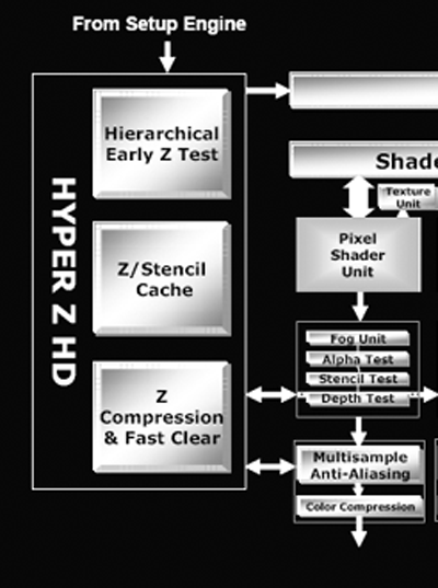
The R420 architecture implements a hierarchical and early z type of occlusion culling in the rendering pipeline.
With early z, as data emerges from the geometry processing portion of the GPU, it is possible to skip further rendering large portions of the scene that are occluded (or covered) by other geometry. In this way, pixels that won't be seen don't need to run through the pixel shader pipelines and waste precious resources.
Hierarchical z indicates that large blocks of pixels are checked and thrown out if the entire tile is occluded. In R420, these tiles are the very same ones output by the geometry and setup engine. If only part of a tile is occluded, smaller subsections are checked and thrown out if possible. This processing doesn't eliminate all the occluded pixels, so pixels coming out of the pixel pipelines also need to be tested for visibility before they are drawn to the framebuffer. The real difference between R3xx and R420 is in the number of pixels that can be gracefully handled.
As rasterization draws nearer, the ATI and NVIDIA architectures begin to differentiate themselves more. Both claim that they are able to calculate up to 32 z or stencil operations per clock, but the conditions under which this is true are different. NV40 is able to push two z/stencil operations per pixel pipeline during a z or stencil only pass or in other cases when no color data is being dealt with (the color unit in NV40 can work with z/stencil data when no color computation is needed). By contrast, R420 pushes 32 z/stencil operations per clock cycle when antialiasing is enabled (one z/stencil operation can be completed per clock at the end of each pixel pipeline, and one z/stencil operation can be completed inside the multisample AA unit).
The different approaches these architectures take mean that each will excel in different ways when dealing with z or stencil data. Under R420, z/stencil speed will be maximized when antialiasing is enabled and will only see 16 z/stencil operations per clock under non-antialiased rendering. NV40 will achieve maximum z/stencil performance when a z/stencil only pass is performed regardless of the state of antialiasing.
The average case for NV40 will be closer to 16 z/stencil operations per clock, and if users don't run antialiasing on R420 they won't see more than 16 z/stencil operations per clock. Really, if everyone begins to enable antialiasing, R420 will begin to shine in real world situations, and if developers embrace z or stencil only passes (such as in Doom III), NV40 will do very well. The bottom line on which approach is better will be defined by the direction the users and developers take in the future. Will enabling antialiasing win out over running at ultra-high resolutions? Will developers mimic John Carmack and the intensive shadowing capabilities of Doom III? Both scenarios could play out simultaneously, but, really, only time will tell.


95 Comments
View All Comments
413xram - Wednesday, May 5, 2004 - link
They announced they where going to in there release anyway. Later on this summer. Why not now?jensend - Wednesday, May 5, 2004 - link
#61- nuts. 512 mb ram will pull loads more power, put out a lot more heat, cost a great deal more (especially now, since ram prices are sky-high), and give negligible if any performance gains. Heck, even 256 mb is still primarily a marketing gimmick.413xram - Wednesday, May 5, 2004 - link
They (ATI) are using the same technology that their previous cards are using. They pretty much just added more transistors to perform more functions at a higher speed. I am willing to bet my paycheck that they spent no where close to 400 million dollars to run neck and neck with nvidia in performance. I guess "virtually nothing" is an overstatement. My apologies.Phiro - Wednesday, May 5, 2004 - link
Where do you get your info that ATI spent "virtually nothing"?413xram - Wednesday, May 5, 2004 - link
Both cards perform brilliantly. They are truly a huge step in graphics processing. One problem I forsee though,is that Nvidia spent 400 million dollars into development of their new nv40 technology, while ATI spent virtually nothing to have the same performance gains. Economically that is a hard pill for Nvidia to swallow.It is true that Nvidia's card has the 3.0 pixel shading, unfortunatly though, they are banking on hardware that is not supported upon release of the card. In dealing with video cards from a consumers standpoint that is a hard sell. I have learned from the past that future possibilties of technology in hardware does nothing for me today. Not to mention the power supply issue that does not help neither.
Nvidia must find a way to get better performance out of their new card, I can't believe I'am saying that after seeing the specs that it already performs at, or it may be a long, HOT, and expensive summer for them.
P.S. Nvidia. A little advice. Speed up the release on your 512 mb card. That would definetly sell me. Overclocking your 6800 is something that 90% of us in this forum would do anyway.
theIrish1 - Wednesday, May 5, 2004 - link
heh, whatever.. whatever, and whatever. I love the fanboyisms....
I admit I am a fan of ATI cards. I bought a 9700pro and a 9500pro(in my secondary gaming rig) when they first came out, and an 8500 "pro" before that...but now I want to upgrade again. I am keeping an open mind. After looking at benchmarks, it is clear the both cards have their wins and losses depending on the test. I don't think there is a clear cut winner. nVidia got there by new innovation/technology. ATI got there by optimizing "older" technology.
At this point, with pricing being the same.. I think I still have to lean to the ATI cards. Main reasons being heat & power consumption. If the 6800U was $75 or $100 cheaper, I would probably go with that. It will be interesting to see where the 6850 falls benchmark wise, and also in pricing. If the 6850 takes the $500 pricepoint, where will that leave the 6800U? $450? Or with the 6850 be $550?
Something else about the x800Pro (which by the way, alot of the readers/posters seem to be getting confused as to what they are talking about between the Pro and XT models). Anyway, there are a few online stores out there taking pre-orders still for the x800PRO.... for $500+. I thought the Pro was going to go at $400 and the XT at $500...?!?
413xram - Wednesday, May 5, 2004 - link
Pumpkinierre - Wednesday, May 5, 2004 - link
On the fabrication o the two Gpus- the tech report:"Regardless, transistor counts are less important, in reality, than die size, and we can measure that. ATI's chips are manufactured by TSMC on a 0.13-micron, low-k "Black Diamond" process. The use of a low-capacitance dielectric can reduce crosstalk and allow a chip to run at higher speeds with less power consumption. NVIDIA's NV40, meanwhile, is manufactured by IBM on its 0.13-micron fab process, though without the benefit of a low-k dielectric."
The extra transistors of the 6800U might be taken up with the cinematic encoding/rendering embedded chip. Although ATI claim encoding in their X800p/XT blurb, I havent seen much yet to distinguish it from the 9800p in this field. The Tech report checked power consumption at the wall for their test systems and the 6800s ramp up the power a lot quicker with gpu speed so I'm not too hopeful about the overclock to 520Mhz and 6800u extreme gpu yields. Still, maybe a new stepping or 90nm SOI shrink might help (I noticed both manufacturers shied away from 90nm).
Anyway brilliant video cards from North America. Congratulations ATI and Nvidia!
NullSubroutine - Wednesday, May 5, 2004 - link
If it was nice sarcasm I can laugh, if it was nasty sarcasm you can back off. I can see it would be simple for me to overlook the map used, however no indication to what Atech used. One could assume or someone could ask for the real answer and if they are really lucky they will get a smart ass remark.After checking through 10 different reviews I found similar results to Atech when they had 25 bots, THG had none.
Next time save us both the hassle and just say THG didnt use bots, and Atech probably did.
TrogdorJW - Tuesday, May 4, 2004 - link
#54 - Think about things for a minute. Gee... I wonder why THG and AT got such different scores on UT2K4.... Might it be something like the selection of map and the demo used? Nah, that would be too simple. /sarcasmFrom THG: "For our tests in UT2004 we used our own timedemo on the map Assault-Torlan (no bots). All quality options are set to maximum."
No clear indication of what was used for the map or demo on AT, but I'm pretty sure that it was also a home-brewed demo, and likely on a different map and perhaps with a different number of players. Clearly, though, it was not the same demo as THG used... unless THG is in the habit of giving their benchmarking demos out? Didn't think so.
I see questions like this all the time. Unless two sites use the exact same settings, it's almost impossible to directly compare their scores. There is no conspiracy, though. Both sites pretty much say the same thing: close match, with the edge going to ATI right now, especially in DX9, while NV still reigns supreme in OGL.