Arm's Cortex-A76 CPU Unveiled: Taking Aim at the Top for 7nm
by Andrei Frumusanu on May 31, 2018 3:01 PM EST- Posted in
- CPUs
- Arm
- Smartphones
- Mobile
- SoCs
- Cortex-A76
Cortex A76 µarch - Backend
Switching to the back-end of the core we have a look at the execution core.

The integer core contains 6 issue queues and execution ports (4 depicted in the slide plus 2 load/store pipelines). There are 3 integer execution pipelines – two ALUs capable of simple arithmetic operations and a complex pipeline handling also multiplication, division and CRC ops. The three integer pipelines are served by 16 deep issue queues. The same size issue queue can also be found serving the single branch execution port.
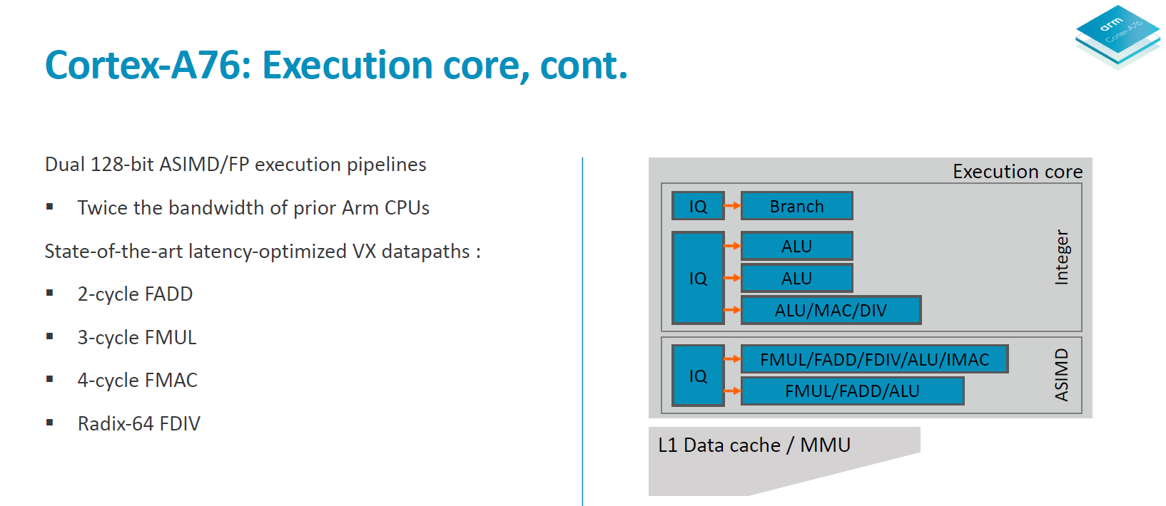
Two load/store units are the remaining ports of the integer core and are each served by two 12 deep issue queues. The issue queue stages are 3 cycles deep and while I mentioned that the rename/dispatch is 1 stage deep, the dispatch stage actually overlaps with the first cycle of the issue queues stages.
The ASIMD/floating point core contains two pipelines which are served by two 16-deep issue queues.
When it comes to the backend of a CPU core the two most important metrics are instruction throughput and latency. Where the A76 in particular improves a lot is in terms of instruction latency as it’s able to shave off cycles on very important instructions.
To better overview the improvements I created a table with the most common instruction types. The execution throughput and latencies presented here are for AArch64 instructions and if not otherwise noted represent operations on 64-bit data for integer and 64bit (double precision) FP.
| Backend Execution Throughput and Latency | ||||||
| Cortex-A75 | Cortex-A76 | Exynos-M3 | ||||
| Exec | Lat | Exec | Lat | Exec | Lat | |
| Integer Arithmetic (Add, sub) | 2 | 1 | 3 | 1 | 4 | 1 |
| Integer Multiply 32b | 1 | 3 | 1 | 2 | 2 | 3 |
| Integer Multiply 64b | 1 | 3 | 1 | 2 | 1 (2x 0.5) |
4 |
| Integer Multiply Accumulate | 1 | 3 | 1 | 2 | 1 | 3 |
| Integer Division 32b | 0.25 | 12 | 0.2 | < 12 | 1/12 - 1 | < 12 |
| Integer Division 64b | 0.25 | 12 | 0.2 | < 12 | 1/21 - 1 | < 21 |
| Move (Mov) | 2 | 1 | 3 | 1 | 3 | 1 |
| Shift ops (Lsl) | 2 | 1 | 3 | 1 | 3 | 1 |
| Load instructions | 2 | 4 | 2 | 4 | 2 | 4 |
| Store instructions | 2 | 1 | 2 | 1 | 1 | 1 |
| FP Arithmetic | 2 | 3 | 2 | 2 | 3 | 2 |
| FP Multiply | 2 | 3 | 2 | 3 | 3 | 4 |
| FP Multiply Accumulate | 2 | 5 | 2 | 4 | 3 | 4 |
| FP Division (S-form) | 0.2-0.33 | 6-10 | 0.66 | 7 | >0.16 (2x 1+/12) |
12 |
| FP Load | 2 | 5 | 2 | 5 | 2 | 5 |
| FP Store | 2 | 1-N | 2 | 2 | 2 | 1 |
| ASIMD Arithmetic | 2 | 3 | 2 | 2 | 3 | 1 |
| ASIMD Multiply | 1 | 4 | 1 | 4 | 1 | 3 |
| ASIMD Multiply Accumulate | 1 | 4 | 1 | 4 | 1 | 3 |
| ASIMD FP Arithmetic | 2 | 3 | 2 | 2 | 3 | 2 |
| ASIMD FP Multiply | 2 | 3 | 2 | 3 | 1 | 3 |
| ASIMD FP Chained MAC (VMLA) | 2 | 6 | 2 | 5 | 3 | 5 |
| ASIMD FP Fused MAC (VFMA) | 2 | 5 | 2 | 4 | 3 | 4 |
On the integer operations side the A76 improves the multiplication and multiply accumulate latencies from 3 cycles down to 2 cycles, with the throughput remaining the same when compared to the A75. Obviously because the A76 has 3 integer pipelines simple arithmetic operations see a 50% increase in throughput versus the A75’s 2 pipelines.
The much larger and important improvements can be found in the “VX” (vector execution) pipelines which are in charge of FP and ASIMD operations. Arm calls the new pipeline a “state-of-the-art” design and this is finally the result that’s been hyped up for several years now.
Floating point arithmetic operations have been reduced in latency from 3 cycles down to 2 cycles, and multiply accumulate has also shaved off a cycle from 5 cycles down to 4.
What Arm means by the “Dual 128bit ASIMD” with doubled execution bandwidth is that for the A75 and prior only one of the vector pipelines was capable of 128bit while the other one was still 64-bit. For the A76 both vector pipelines are 128-bit now so quad-precision operations see a doubling of the execution throughput.
Moving onto more details of the data handling side, we see the again the two load/store pipelines which was something first implemented on the A73 and A75. Although depicted as one issue queue in the slide, the LD/S pipelines each have their own queues at 16 entries deep.
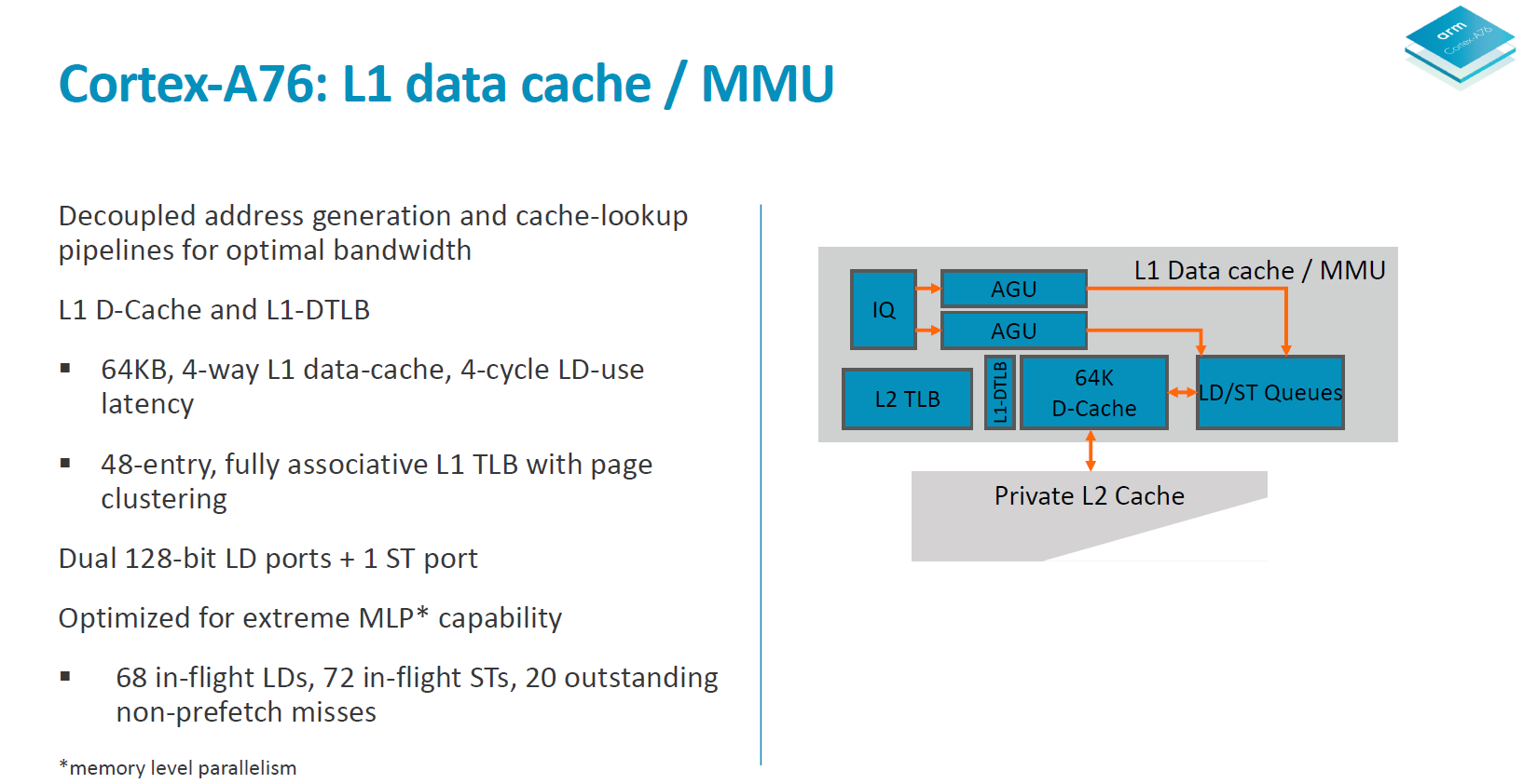
The data cache is fixed at 64KB and is 4-way associative. Load latency remains at 4 cycles. The DTLBs run a separate pipeline as tag and data lookup. Arm’s goals here is aiming for maximum MLP/ memory level parallelism to be able to feed the core.
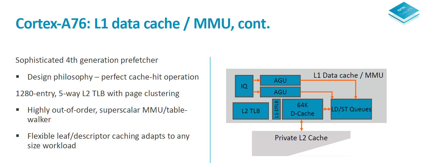
In a perfect machine everything would be already located in the caches, so it’s important to have very robust prefetching capabilities. On the A76 we see a new 4th generation prefetchers introduced to get nearer to this goal of perfect cache-hit operation. In all the A76 has 4 different prefetching engines running in parallel looking at various data patterns and loading data into the caches.
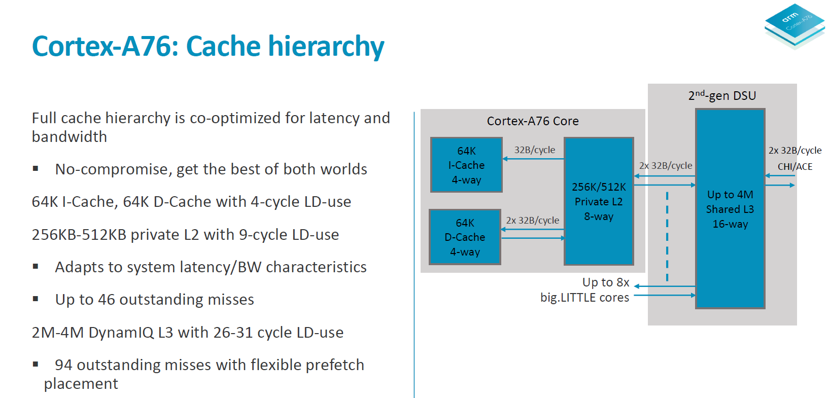
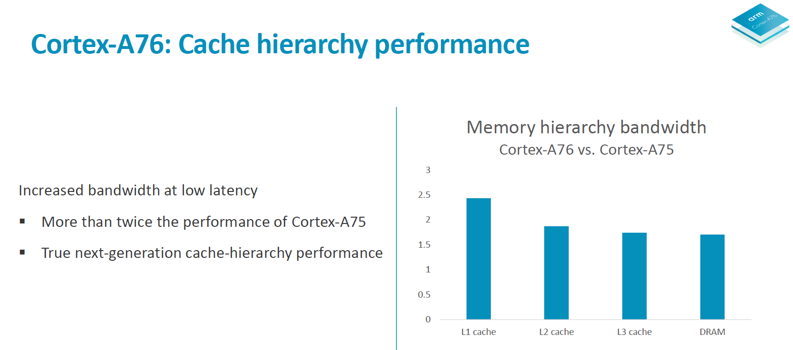
In terms of the A76 cache hierarchy Arm is said to have made no compromises and got the best of both worlds in terms of bandwidth and latency. The 64KB L1 instruction cache reads up to 32B/cycle and the same bandwidth applies to the L1 data cache in both directions. The L1 is a writeback cache. The L2 cache is configurable in 256 or 512KB sizes and is D-side inclusive with the same 2x 32B/cycle write and read interfaces up to the exclusive L3 cache in the 2nd generation DSU.
Overall the microarchitectural improvements on the core are said to improve memory bandwidth to DRAM by up to 90% in microbenchmarks.
All in all the microarchitecture of the A76 could be summed up in a few focus design points: Maximise memory performance throughout the core by looking at every single cycle. During the design phase the engineers were looking at feature changes with a sensitivity of up to 0.25% in performance or power – if that metric was fulfilled then it was deemed to be a worthwhile change in the core. Small percentages then in turn add up to create significant figures in the end product.
The focus on bandwidth on latency is said to have been extreme, and Arm was very adamant in re-iterating that to be able to take full advantage of the microarchitecture that vendors need to implement an equally capable memory subsystem on the SoC to see full advantages. A figure that was put out there was 0.25% of performance per nanosecond of latency to main memory. As we’ve seen in the Snapdragon 845 one of the reasons the SoC didn’t quite reach Arm’s projected performance metrics was the degraded memory latency figures which might have been introduced by the L4 system cache in the SoC. In the future vendors will need to focus more on providing latency sensitive memory subsystems as otherwise they’ll be letting free performance and power on the table with differences that could amount to basically a generational difference in CPU IP.


123 Comments
View All Comments
serendip - Thursday, May 31, 2018 - link
Does anyone actually use the full performance of the A11 or A12 in daily tasks? To me, it's pointless to have a power hungry and fast core just for benchmarks. Just make a slightly slower core with less power usage for quick bursts like app loading or Web page rendering, while much slower and more efficient cores handle the usual workload.jOHEI - Thursday, May 31, 2018 - link
ARM's objectives is to make CPU's that go into a cluster of 4+ another 4 small ones.What Apple has does is Making bigger cores >2 times the size of an ARM core and have 1.5x the performance of the Said core. That same CPU is made for very high Power consumption at maximum load and Apple tweaks the ammount of time it stays in those high clocks. Thus its easier to make a laptop chip-tablet and phone. Because you just reuse the same CPU for all of them, maybe add a few cores to the laptop version and tweak the power settings and its relatively easy.
jOHEI - Thursday, May 31, 2018 - link
Forgot to mention that Apple goes for 2 core clusters, not 4. So they must have significantly better single core performance to matchup against the Conpetition.name99 - Friday, June 1, 2018 - link
Just to correct that you are somewhat living in the past with your numbers.ARM no longer cares about 4-sized clusters; that was an artifact of big.LITTLE (and one of the constraints that limited that architecture's performance). The successor to big.LITTLE, brand-named dynamIQ, does not do things in blocks of 4 anymore.
Likewise Apple first released 3 CPUs in a SoC with the A8X. The A10X likewise has three CPUs. It's entirely likely (though no-one knows for sure) that the A11X (or A12X if the 11X is skipped) will have 4 large cores.
BurntMyBacon - Friday, June 1, 2018 - link
Due to ARM's licensing model, they have every incentive to push designs that cater to more cores. They have little incentive to push single threaded performance any more than necessary as this would result in few cores being licensed due to space and power constraints. I'm not fully convinced that the whole big.LITTLE (and derivative) philosophy was the best way to go either. It could be that it got close enough to what advanced power management could do with the benefit of providing a convincing case for ARM CPU designers to use double the cores or more. When Intel was still in the market, they demonstrated that a dual core chip with clock gating, power gating, power monitoring, dynamic voltage and frequency scaling, and other advanced power management features could provide superior single thread performance and comparable multithread performance in a similar power envelop to competing ARM designs with double the cores (all while burdened with the inefficient x86 decoder). Apple also had good success employing a similar philosophy until their A10 design. Though, it is not necessarily causal, it is interesting to note that they've had more trouble keeping within their thermal and power constraints on their latest A11 big.LITTLE design.Note: I don't have any issue with asymmetric / heterogeneous CPUs. I'm just not convinced that they are adequate replacements for good power management built into the cores. DynamIQ does seem to be a push in the right direction allowing simultaneous usage of all cores, providing hooks for accelerators, and providing fine grained dynamic voltage and frequency scaling. This makes a lot of sense when you can assign tasks to processors (or accelerators) with significantly better proficiency for the task in question. Switching processors for no other reason than it is lower power, however, just sounds like the design team had no incentive to further optimize their power management on the high performance core.
name99 - Friday, June 1, 2018 - link
Again a correction.Apple's problems with the A10 and A11 are NOT problems of power management; they are problems of CURRENT DRAW. Power management on the chips works just fine (and better than ever; high performance throttling tends to occur less with each successive generation, and it used to be possible to force reboot an iPhone if you got it hot enough, now that seems impossible because of better power management).
Current draw, on the other hand, is not something the SoCs were designed to track. And so when an aging battery is no longer able to provide max current draw (when everything on the SoC is lined up just wrong) then not enough current IS provided, and the system reboots.
This is definitely a flaw in the phone as a whole, but it's a system-wide flaw, and you can imagine how it happened. The SoC was designed assuming a certain current drive because no-one thought about aging batteries, because no-one (in Apple or outside) had hit the problem before.
I expect the A12 will have the same PMU that, today, monitors temperatures everywhere to make sure they remain within bounds, ALSO tracking a variety of proxies for current draw, and will be capable of throttling performance gradually in the face of extreme current draw, just like performance is throttled gradually in the face of extreme temperature.
eastcoast_pete - Friday, June 1, 2018 - link
Different design and use philosophies. Apple's mobile chips are designed to be able to deliver short bursts of very high processing power (opening a complex webpage, switching between apps), and throttle back to Okay fast during the remainder. That requires apps and OS to be tightly controlled and behave really well - one bad app that doesn't behave and keeps driving the CPU hard for longer periods and your phone would get hot (thermal throttling) , plus your battery would run down in a jiffy. For ARM & Co on Android/Linux, it makes more sense to have smaller, less powerful cores, manage energy consumption through other means (BigLittle etc), and increase performance by increading the number of cores/threads. Basically, if you really want to upscale the performance of stock ARM designs for a laptop or similar, you could dump the "little" cores and go for an octacore or decacore BIG, so all A76 cores. Might be interesting if somebody tries it.serendip - Friday, June 1, 2018 - link
It's not so simple - small A55 cores seem to work better in a quad or hexacore config, whereas A75s are best left in a dual core config at most because their perf/watt is poor. No point having a phone that's crazy fast but overheats and runs out of battery quickly.Apple's use of powerful but power-hungry cores could also affect the longevity of older phones. Older batteries might not be able to supply enough power for a big core running at full speed.
BurntMyBacon - Friday, June 1, 2018 - link
The fact that Apple is able to use an even larger and more power hungry core and a (marginally?) smaller battery should tell you that it is doable. Though, you are correct in saying it's not simple. The fact of the matter is, Apple has implemented much better power management features than ARM to allow for their cores to run at higher peak loads while needed and then being able to throttle down to lower power draw very quickly. ARM simply didn't design the A75 to do low power processing. The A75 is designed to rely on the A55 for low power processing as this provides an incentive to sell more core licenses.BillBear - Friday, June 1, 2018 - link
Traditionally, Apple builds a big ass core and clocks it low.It wasn't until FinFET made it to mobile chips that they started clocking higher.
>Apple has always played it conservative with clockspeeds in their CPU designs – favoring wide CPUs that don’t need to (or don’t like to) clock higher – so an increase like this is a notable event given the power costs that traditionally come with higher clockspeeds. Based on the underlying manufacturing technology this looks like Apple is cashing in their FinFET dividend, taking advantage of the reduction in operating voltages in order to ratchet up the CPU frequency. This makes a great deal of sense for Apple (architectural improvements only get harder), but at the same time given that Apple is reaching the far edge of the performance curve I suspect this may be the last time we see a 25%+ clockspeed increase in a single generation with an Apple SoC.
https://www.anandtech.com/show/9686/the-apple-ipho...
Qualcomm has been building small cores and vendors have been clocking them (with corresponding voltage increases) high.
Remember all the Android vendors getting caught red handed changing clockspeeds when they detected benchmarks running?