Arm's Cortex-A76 CPU Unveiled: Taking Aim at the Top for 7nm
by Andrei Frumusanu on May 31, 2018 3:01 PM EST- Posted in
- CPUs
- Arm
- Smartphones
- Mobile
- SoCs
- Cortex-A76
Performance & Power Projections
Now that we’ve had more insight into the A76’s microarchitecture – there’s always a disconnect between theoretical performance based on overlying µarch and how it ends up in practice. We’re first going to look at ISO-process and ISO-frequency comparisons which means the generational performance improvements between the cores with otherwise identical factors such as memory subsystems.
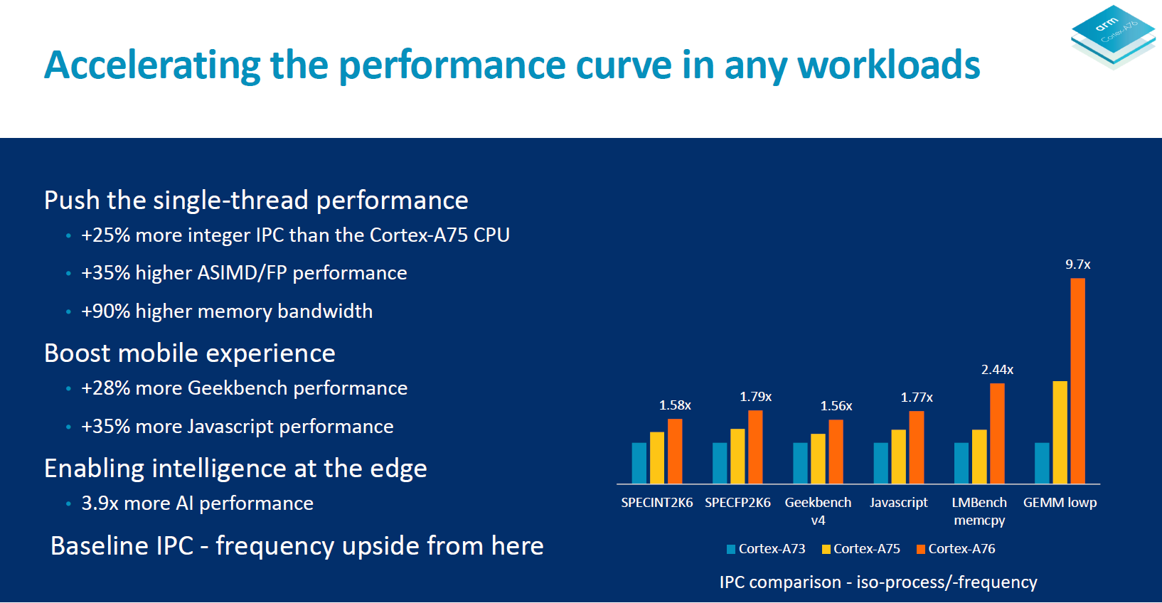
In terms of general IPC Arm promises a ~25% increase in integer workloads and a ~35% increase in ASIMD/floating point workloads. Together with up to 90% higher memory bandwidth figures compared to the A75 the A76 is then meant to provide around a 28% increase in GeekBench4 and 35% more JavaScript performance (Octane, JetStream). In AI inferencing workloads the doubled ASIMD 128-bit capabilities of the A76 serves to quadruple the general matrix multiply performance in half precision formats.
These performance figures are respectable but not quite earth-shattering considering the tone of the improvements of the µarch. However it’s to note that we’re expecting the A76 to come first be deployed in flagship SoCs on TSMC’s 7nm process which allows for increased clocks.
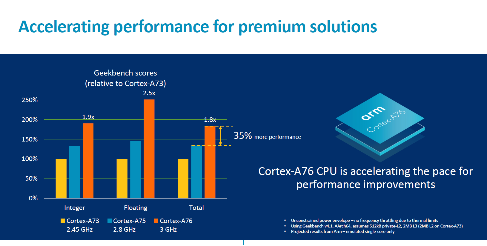
Here Arm’s projections is that we’ll be seeing the A76 clocked at up to 3GHz on 7nm, which in turn will result in higher improvements. Quoted figures are 1.9x in integer and 2.5x in floating point subscores of GeekBench4 while we should be expecting total score increases of 35%.
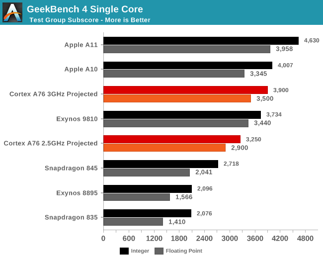
What this means in terms of absolute numbers is projected in the above graph. Baselining on the performance of the Snapdragon 835 and Snapdragon 845 a future SoC with an A76, 512KB L2’s and 2MB L3 would fall in around the GeekBench4 performance of the Exynos 9810 depending if the target 3GHz is reached.
In the past Arm has been overly optimistic when releasing frequency targets – for example the A73 was first projected at up to 2.8GHz and the Cortex A75 projected at up to 3GHz. In the end both ended up at no higher than 2.45GHz and 2.8GHz.
I’ve talked to a vendor about this and it seems Arm doesn’t take into consideration all corners when doing timing signoff, and in particular vendors have to take into consideration process variations which result in differently binned units, some of which might not reach the target frequencies. As mobile chips generally aren’t performance binned but rather power binned, vendors need to lower the target clock to get sufficient volume for commercialisation which results in slightly reduced clocks compared to what Arm usually talks about.
For the first A76 implementations in mobile devices I’m adamant that we won’t be seeing 3GHz SKUs but rather frequencies around 2.5GHz. Arm is still confident that we’ll see 3GHz SoCs but I’m going to be rather on the conservative side and be talking about 2.5GHz and 3GHz projections alongside each other, with the latter more of a projection of future higher TDP platforms.
Arm also had a slide demonstrating absolute peak performance at frequencies of 3.3GHz. The important thing to note here was that this scenario exceeded 5W and the performance would be reduced to get under that TDP target. It wasn’t clear if this was SoC power or solely CPU power – I’ll follow up with a clarification after I reach out to Arm.

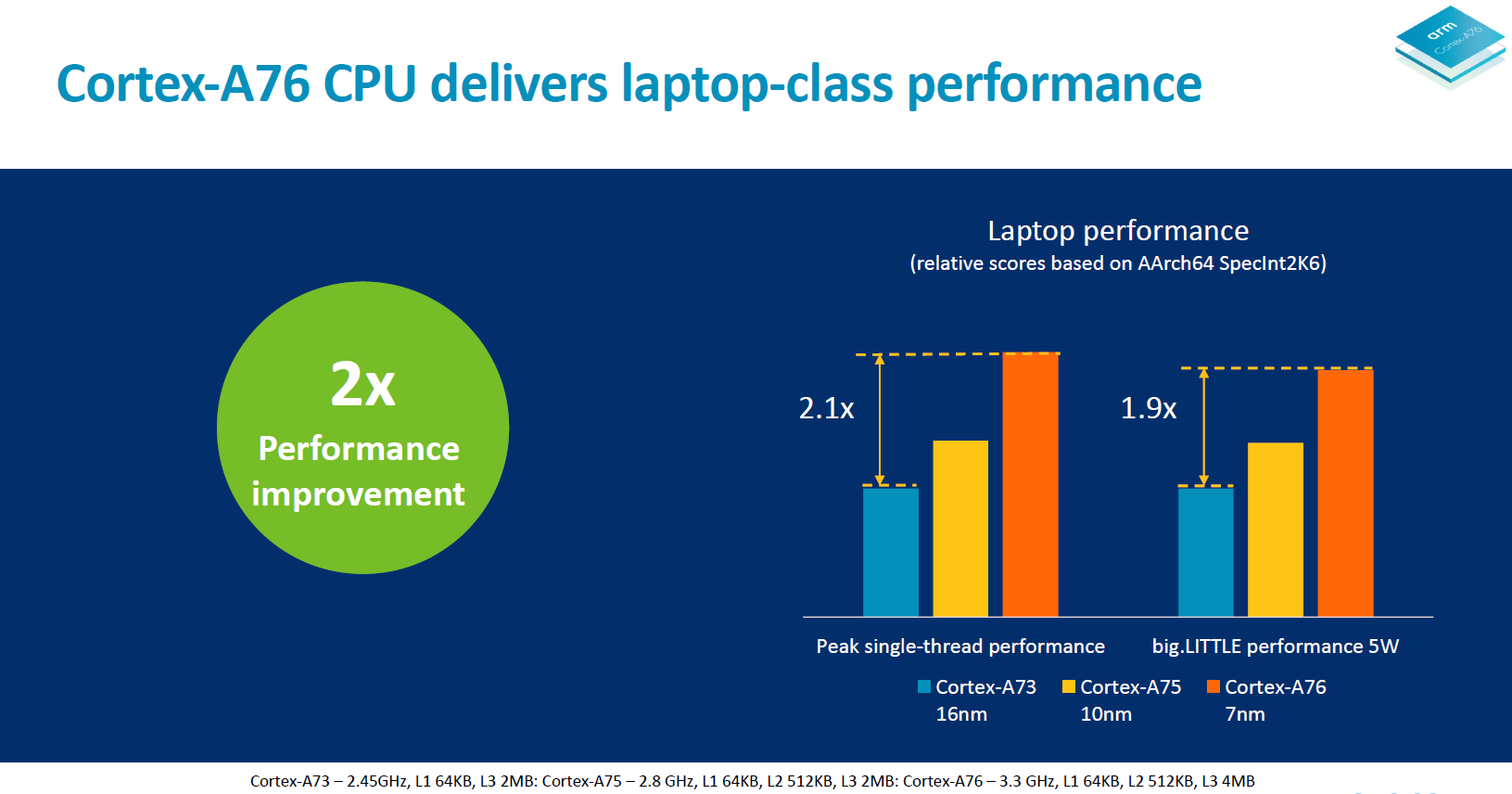
Obviously the most important metric here alongside the performance improvements is the power and efficiency targets. In target products comparing Cortex A75 on a 10nm process versus a Cortex A76 on a 7nm process under the same 750mW/core power budget, the Cortex A76 delivers 40% more performance.
In terms of energy efficiency, a 7nm A76 at a performance target of 20 SPECint2006 of an A75 on 10nm (meaning maximum performance at 2.8GHz) is said to use half the amount of energy.
What is important in all these metrics again is that we weren’t presented an ISO-process comparison or a comparison at maximum performance of the A76 at 3GHz, so we’re left with quite a bit of guesswork in terms of projecting the end energy efficiency difference in products. TSMC promises a 40% drop in power versus 10FF. We haven’t seen an A75 implemented on a TSMC process to date so the best baseline we have is Qualcomm’s Snapdragon 845 on Samsung 10LPP which should slightly outperform 10FF.
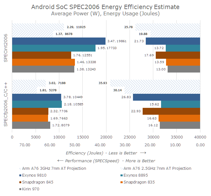
Going through my projected data on one side we have performance on the right side: I baselined the SPECspeed scores on the average of the Snapdragon 835 and Kirin 970 measured results and applied Arm’s projected IPC claims and scaled the scores for frequency. For the 3GHz A76 projection this gets us the near 2x performance improvements in SPECint2006 vs the A73 generation of cores.
In terms of power efficiency, there’s more guesswork as the only real figure we have is as earlier stated the process scaled efficiency figures. Arm quoted a performance target of 20 SPECint2006 which I suspect is a 2.8GHz A75 run with GCC compiled benchmark binaries which have an advantage over my LLVM figures. If Arm wanted to compare against the Snapdragon 845 this matches roughly a 2.4GHz A76. Accounting for the process power improvement this roughly leaves a ~15% microarchitectural advantage for the A76. However as the A76 is targeted to perform 35% higher, and as we’ve seen in the past performance increases through clock don’t scale linearly with power, the power and efficiency advantages would very quickly degrade at peak performance.
Taking all factor into account as best as I could, we should be seeing 7nm A76 based SoCs beat slightly beat the energy efficiency of current Arm SoCs in terms of absolute energy usage at peak performance, a metric which is important as it is directly proportional to a device’s battery life. At a more conservative 2.5GHz clock this energy efficiency advantage would be greater and around 30% less energy than current generation A73 and A75 SoCs.
So on one hand the A76 would be extremely energy efficient, but also it could very well be a thermally constrained design as its peak performance we’d be seeing quite higher TDP figures. Arm states that the A76 is meant to run at full frequency in quad-core mode, however that claim is limited to larger form-factors, as for mobile devices, based on what I’m hearing vendors, will need to tone it down to lower clocks in order to fit smartphone designs.
Again the projection here contain a lot of variables and I’m erring towards the more conservative side in terms of performance and efficiency- however it’s clear that the jump will be significant in whichever way vendors will decide to push the A76 in (Performance or efficiency).


123 Comments
View All Comments
jospoortvliet - Wednesday, June 6, 2018 - link
Twice as fast at half power should not be hard. Of course the process has changed since those chips were baked, it isn't all in architecture.tipoo - Tuesday, September 4, 2018 - link
Yeah, on 7nm they should easily be able to make portable mode do what docked mode did, and add a new higher performance docked mode. Easy transition.name99 - Friday, December 18, 2020 - link
"The branch prediction unit is what Arm calls a first in the industry in adopting a hybrid indirect predictor. "This is somewhat misleading. The fetch unit is very interesting (and Andrei did not spend enough time praising it) but to say that it is first in the industry seems unreasonable.
The idea of decoupling the stream of fetch addresses from actual I-cache access dates from a thesis in 2001. Implementations I know about include Zen and Exynos M1 (2016) and IBM z14 (2017). Apple probably got in there even earlier.
So there may be some very specific detail in how ARM is implementing this that is a first, but the overall idea has been around for 17 years.
(The reason why it's taken so long to be implemented is that, first, it needs lots of transistors to store all the predictor state and, second, it requires some rethinking of how your branch predictors are indexed and updated. Think about it. What you want is machinery that, EVERY CYCLE, when given a PC will spit out two addresses -- where the current run of straightline fetching must end, ie the next TAKEN branch target, and where the PC must be directed to when it hits the end of this basic block. And it has to do this "in isolation", without looking at the instructions that are going to be loaded from the I$ because the whole point is that this is happening decoupled from, and in advance of, access to the I$. It's not trivial to think of a set of data structure that can do that. I'm still not at all convinced my understanding of exactly how this is correct, even though I've been trying to understand it for some time now.)