Assessing Cavium's ThunderX2: The Arm Server Dream Realized At Last
by Johan De Gelas on May 23, 2018 9:00 AM EST- Posted in
- CPUs
- Arm
- Enterprise
- SoCs
- Enterprise CPUs
- ARMv8
- Cavium
- ThunderX
- ThunderX2
ThunderX: From Small & Simple to Wide & Complex
As a brief recap, the original ThunderX was an improved version of the Octeon III: a dual-issue in-order CPU core with two short pipelines.
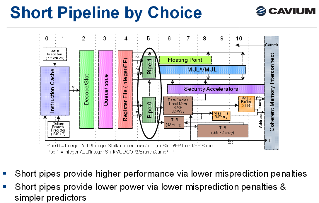
The advantage of the original ThunderX design is that such a simple core can be very energy efficient, especially for "low ILP" (instruction level parallelism) workloads such as web servers and most database servers. Of course, such a short pipeline limits the clockspeed, and such a simple in-order design offers low single threaded performance in medium and high ILP workloads, whereas more advanced out-of-order processors can extract significant parallelism.
Cavium's "New" Core: Vulcan
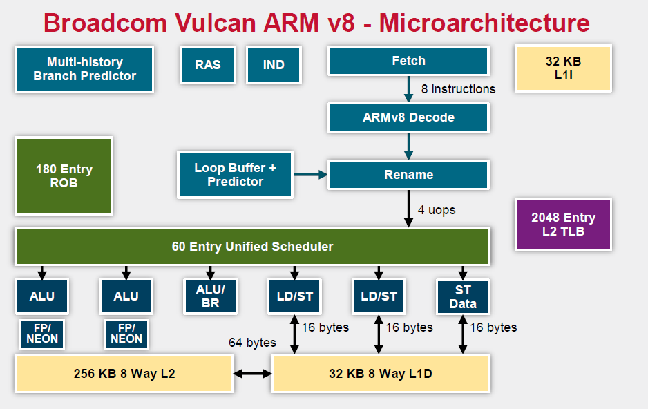
Relative to the original ThunderX, the Vulcan core of the ThunderX2 is an entirely different beast. Announced in 2014 by Broadcom, it is a relatively wide core that runs 4 simultaneous threads (SMT4). As a result, the wide back end should be quite busy even when running low-ILP server workloads.
To make sure that all 4 SMT threads can be sustained, the ThunderX2 front-end can fetch up to 64 bytes from the 8-way set associative 32 KB instruction cache, which is outfitted with a simple next line prefetcher. However, fetching 8 instructions is only possible if there is no taken branch inside those 64 bytes. In that case, the fetch breaks off at the taken branch.
That means that in branch intensive code (databases, AI...) the fetcher will get +/- 5 instructions per clock cycle on average, as one out of 5 instructions is a branch. The fetched instructions are then sent to a smoothing buffer – a buffer where the fetched instructions are held for decoding.
The decoder will then work on a bundle of 4 instructions. Between the decoder and the rename phase each thread has "skid buffer" which consists of 8 bundles. So between the 4 threads up to 32 bundles (128 instructions) can be skid buffered at any one time..
Those 4 instructions – a bundle – travel together through the pipeline until they reach the unified issue queue of the scheduler. Just like Intel has implemented in Nehalem, there is also a loop buffer and predictor, which Intel used to call a "Loop Stream Detector". This loop buffer avoids branch mispredictions and contains decoded µops, which "shortens" the pipeline and reduces the amount of power spent on decoding.
Overall, up to 6 instructions can be executed at the same time. This is divided into 2 ALU/FP/NEON slots, 1 ALU/branch slot, 2 load/store slots (16 bytes), and 1 pure store slot that sends 16 bytes to the D-cache. There is a small (Cavium would not disclose how small) L1 TLB for zero latency translation from Virtual to physical addresses. There is no hardware prefetcher for the L1 D-cache, but the L2 cache has a rather complex hardware prefetcher which is able to recognize patterns (besides being able to stride or fetching the next line).
This is enough to feed the back-end, which can sustain 4 instructions per cycle from 4 different threads.
Micro Architecture Differences
Ultimately Cavium has only published a limited amount of information on the ThunderX2 cores, so there are some limits to our knowledge. But we've gone ahead and summarized some of the key specifications of the different CPU architectures below.
| Feature | Cavium ThunderX2 |
Qualcomm Centriq "Falkor" |
Intel "Skylake"-SP |
AMD EPYC "Zen" |
| L1-I cache Associativity |
32 KB 8-way |
64KB 8-way (+ 24 KB L0) |
32 KB 8-way |
64KB 4-way |
| L1-D cache Associativity |
32 KB 8-way |
32 KB 8-way* |
32 KB 8-way |
32 KB 8-way |
| Load Bandwith | 2x 16B | 2x 16B | 2x 32B | 2x 16B |
| L2-cache | 256 KB 8-way |
256 KB 8-way |
1 MB 16-way |
512 KB 8-way |
| Fetch Width | 8 instructions | 4 instructions | 16 bytes (+/- 4-5 x86) | 32 bytes (+/- 6-8 x86) |
| Issue Queue | 60 | 76 | 97 unified | 6x14 |
| Sustainable Instructions/cycle | 4 | 4 | 5-6 | 4-5 |
| Instructions in Flight | 180 (ROB) | 128 | 224 (ROB) | 192 |
| Int. Pipeline Length |
? |
15 stages | 19 stages 14 stage from µop cache |
19 stages? |
| TLB Instructions TLB Data |
"Small L1" + 2048 unified L2 | ? 64+512 |
128 64 +1536 Unified |
8+64+512 64+1532 |
A detailed analysis is out of the scope of this article. But you can read Ian's analyses of the Falkor, Skylake and Zen architectures here at AnandTech. We limit ourselves to the most obvious differences.
It is pretty clear that Intel's single-threaded performance remains unchallenged: the Skylake core is the widest core, keeps the most instructions in flight, and most importantly runs at the highest clockspeed. The ThunderX2 core is the one that fetches the most instructions per cycle, as it has to be able to keep 4 threads running. The fetch unit will grab 8 instructions from one thread, than grab 8 from the second thread and it will keep cycling between threads. A bad prediction could thus lower the performance of single thread significantly.


97 Comments
View All Comments
Wilco1 - Wednesday, May 23, 2018 - link
You might want to study RISC and CISC first before making any claims. RISC doesn't use more instructions than CISC. Vector instructions are actually quite similar on most ISAs. In fact I would say the Neon ones are more powerful and more general due to being well designed rather than added ad-hoc.HStewart - Wednesday, May 23, 2018 - link
The following site explain the difference using a simple multiply action, where a CISC architecture can do in single instruction, RISC would need to use multiple instructionshttp://www.firmcodes.com/difference-risc-sics-arch...
of course as time move on RISC chips added more complex operations and CISC also found ways to breaking more complex CISC instruction in smaller RISC like microcode increasing the chip ability to multitask the pipeline.
Wilco1 - Thursday, May 24, 2018 - link
The example was about load/store architecture, not multiply. In reality almost all instructions use registers (even on CISCs) since memory is too slow, so it's not a good example of what happens in actual code. The number of executed instructions on large applications is actually very close. The key reason is that compilers avoid all the complex instructions on x86 and mostly use register operations, not memory.Kevin G - Tuesday, May 29, 2018 - link
Raw instruction counts isn't a good metric to determine the difference between RISC and CISC, especially as both have evolved to include various SIMD and transactional extensions.The big thing for RISC is that it only supports a handful of instruction formats, generally all of the same length (traditionally 4 bytes)* and have alignment rules in place. x86 on the other hand leverages a series of prefixes to enhance instructions which permits length up to 15 bytes. On the flip side, there are also x86 instructions that consume a single byte. This also means x86 doesn't have the alignment rules that RISC chips generally adhere to.
*ARM does offer some compressed instruction formats in Thumb/Thumb2 but they those are also of a fixed length. 16 bit Thumb instructions are half size as 32 bit ARM instructions and have alignment rules as well.
Modern x86 is radically different internally than its philosophical lineage. x86 instructions are broken down into micro-ops which are RISC-like in nature. These decoded instructions are now being cached to bypass the complex and power hungry decode stages. Compare this to some ARM cores where some instructions do not have to be decoded. While having a simpler decode doesn't directly help with performance, it does impact power consumption.
However, I would differ and say that ARM's FPU and vector history has been rather troubled. Initially ARM didn't specify a FPU but rather a method to add coprocessors. This lead to 3rd parties producing ARM cores with incompatible FPUs. It wasn't until recently that ARM themselves put their foot down and mandated NEON as the one to rule them all, especially in 64 bit mode.
peevee - Wednesday, May 23, 2018 - link
The whole RISC vs CISC distinction is outdated for at least 20 years. Both now include a shi(p)load of instruction far outnumbering original CISC processors like 68000 and 8088 (from the epoch of the whole CISC vs RISC discussion), and both have a lot of architectural registers (which on speculative OoO CPUs are not even the same as real register files). ARMv8 for example includes NEON instructions, which is like... "AVX-128" (or SSE3 or smth).A lot of instructions means that both have to have huge decoders, which limits how small the CPU can be (because any reduction in other hardware which decrease performance faster than cost). For 64-bit ARMv8.2 it is very unlikely than an implementation can be made smaller than A55, and it is a huge core (in transistors) compared to even Pentium, let alone 8088.
HStewart - Wednesday, May 23, 2018 - link
I think the big difference between SIMD technologies - even though ARM has included they are not as wide as instructions as Intel or AMD. The following link appears to have a good comparison of chip SIMD comparison in size, To me in looks like AMD is on AVX level 8/16 instead of 16/32 in current chips while ARM including Neon is 4 Wide which is actually less than Core 2 SSE instructions from 10 years ago.https://stackoverflow.com/questions/15655835/flops...
It also interesting to note Ryzen stats - which I heard that AMD implement AVX 256 by combine two 128 together
One thing is that both Intel and AMD CPUs have grown a long ways since 20 years ago. In fact even todays Atom's can out rune most core-2 CPU's from 10 years - not my Xeon 5160 however.
ZolaIII - Thursday, May 24, 2018 - link
It's 2x128 NEON SIMD per ARM A75 core which goes into your smartphone.Even with smaller SIMD utilising TBL QC Centriq is able to beat up an Xerox Gold.
https://blog.cloudflare.com/neon-is-the-new-black/
Wilco1 - Thursday, May 24, 2018 - link
Modern Arm cores have 2-3 128-bit SIMD units, so 16-24 SP FLOPS/cycle. About half of Skylake theoretical flops, and yet they can match or beat Skylake on many HPC codes. Size is not everything...peevee - Thursday, May 24, 2018 - link
"ARM including Neon is 4 Wide which is actually less than Core 2 SSE instructions from 10 years ago"How is it less? It is the same 128 bits, 2x64 or 4x32 or 2x16...
And AMD combines 2 AVX-256 operations (not 2 128-bit SSEs) to get AVX-512.
patrickjp93 - Friday, May 25, 2018 - link
AMD does NOT have AVX-512. They combine 2 128s into a 256 on Ryzen, ThreadRipper, and Epyc.