Power Stamp Alliance Exposes Ice Lake Xeon Details: LGA4189 and 8-Channel Memory
by Ian Cutress on April 9, 2018 11:42 AM EST
For everyone waiting for Cascade Lake, Intel’s next server Xeon platform, to be launched, noise is being made from the Power Stamp Alliance and its members about the platform beyond Cascade Lake. Alliance member Bel Power Solutions, along with the Power Stamp website, have exposed several details on the Ice Lake Xeon platform.
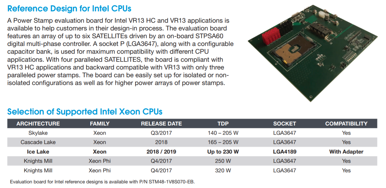
The first element of the information is the new socket, set at LGA4189. This is compared to the current Xeon socket, standing at LGA3647, which currently supports the Skylake Xeon family as well as the upcoming Cascade Lake Xeon family. According to the documents, the power pin implementation between the new LGA4189 and LGA3647 sockets are compatible via an adaptor: this isn’t to say the CPUs themselves will be, but it would appear that all the Skylake/Cascade Lake/Ice Lake Xeon families will have a similar power implementation. The reason why we mention the power implementation only is because the Power Stamp Alliance (and Bel Power Solutions) is only dealing with DC-to-DC converters for the platforms, driving efficiency from a high 48V input correlating with the Open Compute Project (OCP) standards and deployments.

Also in this image (and verified at Power Stamp) are the power ranges for Cascade Lake (165-205W, similar to Skylake Xeons) and for Ice Lake (set to go to 230W). Should the new Ice Lake Xeon platform incorporate features such as OmniPath or on-package FPGAs, which Intel has teased future Xeon platforms to be, then 230W is well within the reasons of possibility. Also, having a high DC-to-DC efficiency is going to assist with overall power consumption and power loss.
Delving into the documents, the Power Stamp Alliance designates two code names in play: VR13 (for Skylake and Cascade Lake) and VR13-HC (for Ice Lake). The HC in this case stands for high-current, and the documentation shows ‘a typical’ VR13-HC implementation with two CPUs and sixteen DDR4 memory slots for each CPU. The Bel Power systems documents goes on to say that a VR13-HC system (Ice Lake) with four power stamps meets the VR13-HC minimum requirements, while only three are needed for VR13 (Skylake/Cascade).
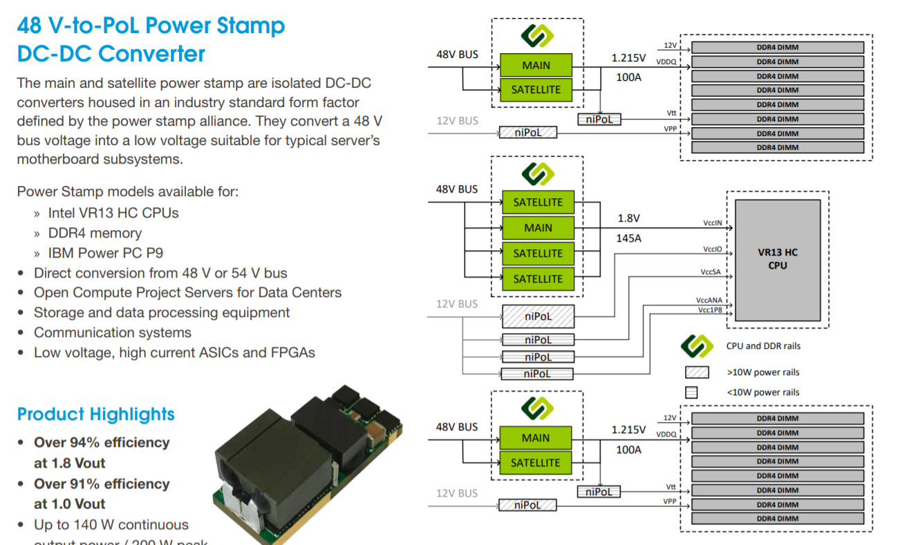
The images shown above and below point to Ice Lake Xeons being equipped with native eight-channel DDR4, given how Intel dropped 3 DIMM per channel support with Skylake. This comes through the chip directly, rather than implementing memory buffers, such as the Jordan Creek implementation on the E7 v4 family. With the 8-channel design, one might assume Intel boosting the maximum memory capacity of the base Xeon processors from 768GB to 1TB, although we should wait to see if that is going to be the case. If Intel is using the same on-chip network implementation as Skylake, it would also mean that one of the segments that previously used for a tri-memory channel controller actually has enough space for a quad-memory channel controller.
No special mention is made regarding XPoint memory support. Parts of the documents state that a set of 8 DRAM slots and two power stamps should be good for 100-200A at 1.215 V for VDDQ, implying that a set of 8 memory sticks should be able to draw around 120W-240W, or ~15-30W each. Varying numbers have been postulated as to the power draw of XPoint modules, but most numbers are within this range.
More information from the Power Stamp Alliance is set to be given at the Open Compute Summit, happening in late May. The Alliance consists of STMicroelectronics, Artesyn Embedded Technologies, Bel Power Solutions, and Flex
Sources: Bel Power Solutions, Power Stamp Alliance, via Twitter
*This article first stated that the OCP Summit was going to happen in Late May. It actually happened in Late March already.


37 Comments
View All Comments
vgray35@hotmail.com - Tuesday, April 10, 2018 - link
Did I mention a 50 kHz DC-DC converter using hybrid PWM-resonant switching and resonance scaling, allows a 48V to 1V conversion ratio at 50% duty cycle and not 2% pulse width as in a Buck converter. The war drums are rolling.iter - Tuesday, April 10, 2018 - link
Waste is not an issue if it can be translated into profit.Even when it wastes critically important finite quantity rare Earth elements.
vgray35@hotmail.com - Wednesday, April 11, 2018 - link
Waste is not the issue - heat is - which translates into a) reduced life of components due to stress, b) increased size and cost of several PSU and VRMs elements, c) trouble providing cooling at a reasonable cost, and of course, d) much larger cost of the board overall. Cost, Cost, Cost, and reduced component life. I would have thought that was obvious in my posting. There is of course noise due to several cooling fans which constantly annoy you. If I can get both reduced noise, and cost, why would I not go for it. Oh yes, and reduced cost also means increased profitability due to better margins, so your point is moot, or at least I fail to see how waste in this case could possibly translate to profitability - it cannot. It has nothing to do with rare Earth elements, just common sense and good business.flgt - Tuesday, April 10, 2018 - link
I would like to see the total cascaded efficiency in a server farm from mains to a 1V processor rail before making any opinions. Dealing with any individual stage's efficiency can be misleading.In regards to GaN, I was just saying that IN THEORY it should have better performance at any given switching frequency than silicon. I agree that running DC-DC converters at 2 MHz to get size down has diminishing returns that even GaN can't overcome.
vgray35@hotmail.com - Wednesday, April 11, 2018 - link
Efficiency varies with load, with both lower and higher loads less than peak efficiency. A good average for Buck converters is 82 - 85% at best. ATX power supply yields 12V, then VRM's use that to provide 1V, and the two cascaded easily result in 40% losses overall. Actually your point about GaN is quite relevant and accurate, as it is superior to Silicon MOSFETs at any frequency. With GaN all the devices could be integrated on a single chip with the driver (already being done by TI for a half bridge), and then enlarge the current flow area to reduce Rdson. Integrate the controller onto the chip too (not done yet), and using a topology that does not require an air-gapped ferrite inductor makes the VRM footprint a tiny fraction of Buck converters. Not to mention a tiny fraction of the cost. The inductor is a 5 mm length of wire to give 10nH air-cored inductance at 50kHz. The efficiency is in the range of 99% to 99.5%, or as low as 98.5% at load currents approaching 200 to 250 Amps. Modern CPUs are already exceeding 150A with server chips up in the 230A range, and at 50kHz switching losses for GaN are moot, and with conduction losses very low by making the transistor current flow region larger in area, unheard of efficiencies are possible. The power supply on a single chip is possible today with GaN and newer switching methods of the newer topologies - compare that with motherboards today with 16 ferrite chokes and as many as 30 chips. A 300 Amp VRM would be very tiny with just a single chip. I would bet VRM cost exceeds 25% of total motherboard cost at the high end, and for servers >30%.iwod - Monday, April 9, 2018 - link
An 8 Channel Design and still only 1TB Memory support?Ian Cutress - Monday, April 9, 2018 - link
Intel split its SKL-SP family into SKUs that supported 768MB and M versions that supported 1536MB for about 30% more. The argument from Intel was that only 5% of the market needed that amount of memory per socket. So following that logic, they might have SKUs supporting 1TB and 2TB, unless they double up all around and go to 2TB/4TB depending on the LRDIMMs available.The_Assimilator - Monday, April 9, 2018 - link
And, of course, Intel charges at least 100% more for the -M chips... that are probably ordinary chips without one bridge cut. Meanwhile AMD's Epyc lineup supports up to 2TB RAM per CPU without any artificial model segmentation.jerrytsao - Monday, April 9, 2018 - link
And E7 v4 was used to support 3DPC at max 3TB per socket (24TB for 8 sockets) via Jordan Creek Scalable Memory Buffer, the reason Intel ditched that 3DPC is because it would operate only at DDR4-1333 for E7 and DDR4-1866 for E5, Skylake-SP can do 2666 in all config (whether 1DPC or 2DPC) no matter how many ranks each DIMM has. EPYC has a much weaker IMC which can only operate 2666 in 1R RDIMM & in 1DPC only, for RDIMM all other configs would drop to 2400 or 2133, LRDIMM would fare better but is much more expensiveduploxxx - Tuesday, April 10, 2018 - link
but EPYC already has 8 dimm/cpu meaning that a dualsocket has already 512GB ram without the need of the second DIMM row. And all SKU -1 drop to 2400 when dual row dimms, marginal perf diff for such a memory layout.