Samsung Starts Mass Production of 16Gb GDDR6 Memory ICs with 18 Gbps I/O Speed
by Anton Shilov on January 18, 2018 9:00 AM EST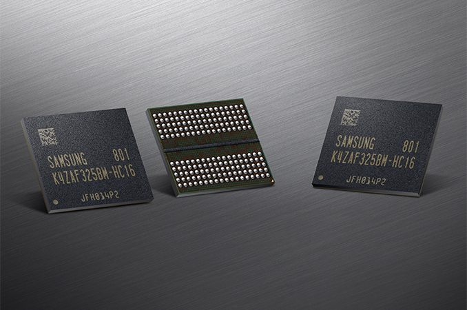
This week, Samsung has announced that it has started mass production of its GDDR6 memory chips for next-generation graphics cards and other applications. The new chips will be available in 16 Gb densities and will feature an interface speed that is significantly higher when compared to that of the fastest GDDR5 and GDDR5X ICs can offer.
GDDR6 is a next-generation specialized DRAM standard that will be supported by all three leading makers of memory. Over time, the industry will introduce a great variety of GDDR6 ICs for different applications, performance and price requirements. What Samsung is announcing this week is its first 16 Gb GDDR6 IC that features an 18 Gbps per pin data transfer rate and offers up to 72 GB/s of bandwidth per chip. A 256-bit memory subsystem comprised of such DRAMs will have a combined memory bandwidth of 576 GB/s, whereas a 384-bit memory subsystem will hit 864 GB/s, outperforming existing HBM2-based 1.7 Gbps/3092-bit memory subsystems that offer up to 652 GB/s. The added expense with GDDR6 will be in the power budget, much like current GDDR5/5X technology.
| GPU Memory Math: GDDR6 vs. HBM2 vs. GDDR5X | ||||||||
| Theoretical GDDR6 256-bit memory sub-system | Theoretical GDDR6 384-bit memory sub-system | NVIDIA Titan V (HBM2) |
NVIDIA Titan Xp |
NVIDIA GeForce GTX 1080 Ti | NVIDIA GeForce GTX 1080 | |||
| Total Capacity | 16 GB | 24 GB | 12 GB | 12 GB | 11 GB | 8 GB | ||
| B/W Per Pin | 18 Gb/s | 1.7 Gb/s | 11.4 Gbps | 11 Gbps | ||||
| Chip capacity | 2 GB (16 Gb) | 4 GB (32 Gb) | 1 GB (8 Gb) | |||||
| No. Chips/KGSDs | 8 | 12 | 3 | 12 | 11 | 8 | ||
| B/W Per Chip/Stack | 72 GB/s | 217.6 GB/s | 45.6 GB/s | 44 GB/s | ||||
| Bus Width | 256-bit | 384-bit | 3092-bit | 384-bit | 352-bit | 256-bit | ||
| Total B/W | 576 GB/s | 864 GB/s | 652.8 GB/s | 547.7 GB/s | 484 GB/s | 352 GB/s | ||
| DRAM Voltage | 1.35 V | 1.2 V (?) | 1.35 V | |||||
The new GDDR6 architecture enables Samsung to support new and higher data transfer rates with non-esoteric memory form factors. To increase the interface speed, GDDR6 memory was redesigned both internally and externally. While details about the new standard will be covered in a separate article, two key things about the new memory tech is that GDDR6 features a x8/x16 per-channel I/O configuration, and each chip now has two channels. By contrast, GDDR5/GDDR5X ICs feature a x16/x32 I/O config as well as one channel per chip. While physically GDDR6 chips continue to feature a 16-/32-bit wide bus, it now works differently when compared to prior generations (as it consists of two channels).
In addition to higher performance, Samsung’s GDDR6 16 Gb chips also operate at 1.35 V voltage, down 13% from 1.55 V required by high-performance GDDR5 ICs (e.g., 9 Gbps, 10 Gbps, etc.). According to Samsung, the lowered voltage enables it to lower energy consumption of GDDR6 components by 35% when compared to ultra-fast GDDR5 chips. Samsung attributes lowered voltage to its new low-power circuit design. Meanwhile, based on information we know from Micron and SK Hynix, their GDDR6 DRAMs will also operate at 1.35 V.
Samsung uses one of its 10nm-class process technology to produce its GDDR6 components. The company claims that its 16 Gb ICs bring about a 30% manufacturing productivity gain compared to its 8 Gb GDDR5 chips made using its 20 nm process technology. Typically, Samsung’s productivity gain means increase in the number of chips per wafer, so the company has managed to make its 16 Gb ICs smaller than its previous-gen 8 Gb ICs. The company does not elaborate on its achievement, but it looks like the new chips are not only made using a thinner process technology, but have other advantages over predecessors, such as a new DRAM cell structure, or an optimized architecture.
Samsung’s 16 Gb GDDR6 chips come in FBGA180 packages, just like all industry-standard GDDR6 memory components from other manufacturers.
Samsung did not disclose when it plans to ship its GDDR6 DRAMs commercially, but since it had already started mass production, it is highly likely that the company’s clients are ready to build products featuring the new memory.
Related Reading
- Micron Finishes GDDR6 Internal Qualification, Eyes H1'2018 Mass Production
- Samsung Starts Production of 8 Gb DDR4-3600 ICs Using 2nd Gen 10nm-Class Tech
- Samsung Pre-Announces 16 Gbps GDDR6 Chips for Next-Gen Graphics Cards
- Micron Discusses GDDR: 16 Gbps GDDR5X, 16 nm GDDR6 and GDDR5
- SK Hynix Advances Graphics DRAM: GDDR6 Added to Catalogue, GDDR5 Gets Faster
Source: Samsung


24 Comments
View All Comments
boeush - Thursday, January 18, 2018 - link
Maybe my math is naive or somehow wrong, but at a first approximation, going from a 20 nm-class process down to a 10-nm class increases the number of circuit elements per unit area by roughly a factor of 4.
So if the density went up by 4x, but the memory capacity went only from 8 Gb to 16 GB (2x), then why wouldn't we expect roughly 2x the number of dies per wafer even with otherwise no other changes?
limitedaccess - Thursday, January 18, 2018 - link
All the DRAM/NAND manufactures are obfuscating the actual designation of their sub 20nm process hence why terms like 10nm class or 1x nm http://www.samsung.com/semiconductor/dram/gddr6/ as opposed to outright stating 10nm. On top of that the process designations from foundries are effectively arbitrary and not subject to any standard independent measurement with respect to actual density of end products.MrSpadge - Thursday, January 18, 2018 - link
The first "10 nm class" NAND processes where 2 generations of 19 nm processes (e.g. Toshiba, if I remember corrctly).Regarding the scaling discussed here: moving from 8 GBit to 16 Gbit dies will reduce the fraction of area for fixed control logic and decrease the area lost to die sawing. Both increase "productivity" in addition to the new process. Besides, "30% higher productivity" has by no means to mean "the new chip is smaller". Otherwise the increase would have to exceeded approximately 100%. The new chip will be larger, but they now get ~30% more DRAM capacity per wafer, i.e. less dies.
martinpw - Thursday, January 18, 2018 - link
Yes indeed, "class" is a weasel word here. "10nm class" just means the first digit is a 1. So anywhere between 10nm and 19nm.FreckledTrout - Thursday, January 18, 2018 - link
LIke limitedaccess said, only the marketing density went up by 4x the actual density is likely closer to 2x.webdoctors - Thursday, January 18, 2018 - link
This is great news. You'd be able to get HBM or better bandwidth for much less BOM costs (no interposer or HBM memory prices to pay) plus better yields since no interposer issue.SunnyNW - Thursday, January 18, 2018 - link
Am I the only one that is extremely impressed by the speed of these ICs, especially being very early in the life cycle? The 18 gbps is even more than the initial announcement of 16 gbps and if I'm not mistaken I believe even the JEDEC spec states the fastest speed for GDDR6 as 16 gbps.MrSpadge - Friday, January 19, 2018 - link
+1