AMD Tech Day at CES: 2018 Roadmap Revealed, with Ryzen APUs, Zen+ on 12nm, Vega on 7nm
by Ian Cutress on February 1, 2018 8:45 AM ESTVega in 2018
One of the more disappointing elements to the roadmap announcements at AMD’s Tech Day was about graphics, and specifically Vega. To put it bluntly, there are no updates from AMD coming to the consumer desktop graphics market in 2018. With everything going on regarding the cycle of GPU architectures, and the insatiable demand for AMD graphics cards from cryptocurrency miners driving prices sky-high, the enthusiast and high-end gamers are getting the thin-end of the wedge.
Unfortunately, AMD is getting the blame for this, with many gamers blindly demanding ‘why not make more?’. In a recent earnings call, AMD CEO Lisa Su that they are making as many Vega graphics processors as possible, and also increasing their order with the fabs to produce more. Dr. Su put the problems with production squarely in the hands of the DRAM manufacturers, stating that memory supplies (GDDR5 and HBM2) are not sufficient to meet the high demand from everyone that needs them, which is also driving up cost. As a result, AMD isn’t blaming itself for the lack of GPUs being made available to consumers, but is saying that Samsung, Micron, and SK Hynix are not producing enough. AMD seem to be selling as many GPUs as they can make, which is good for their balance sheet at least.
So while there is nothing to look forward to on the desktop graphics side, AMD did mark on its roadmap two specific graphics products for 2018.
Vega Mobile, with HBM2
The graphics strategy in notebooks is bifurcated for AMD. On one side, their Mobile APU business takes care of the low-end of the market. The recent business relationship with Intel to sell graphics chips for Intel’s high-end mobile processors means AMD has a business on that side. The big hole in the middle is for notebook customers that want discrete graphics. After a couple of years of large Polaris based designs using GDDR, AMD is bringing Vega to this market.
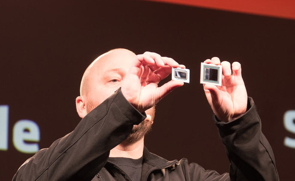
As far as AMD were prepared to announce, a single Vega Mobile design is being prepared, which might be subject to binning based on compute units. The full amount of compute units in the chip has not been made publicly available, however it measures basically half of the full Vega 64 chip next to it. This would normally suggest a 32 CU chip, however there are a number of front-end elements required which have a fixed size – compared to the Intel 24 CU chip for the Intel with Radeon Graphics processor, this chip seems to be of similar size, if not bigger.
What we do know about the Vega Mobile processor is that it is paired with 4GB of HBM2, using an embedded interposer to give an overall z-height of 1.7mm. This is AMD’s second or third generation of interposer technology, and it has come a long way since Fiji: the interposer is tight along the dimensions of the GPU and HBM, but it is also embedded into the PCB. The embedding allows it to reduce the height, making it a better fit for ‘thin and light’ mobile platforms. The interesting correlation here is that at 1.7mm, it matches Intel’s EMIB implementation which is also 1.7mm. This caused two theories: either AMD is using EMIB (it isn’t), or it means that the perceived z-height benefit from using EMIB might not exist. The latter is true: AMD has unequivocally confirmed that it is using an interposer, and does not have access to Intel’s EMIB.
Ultimately AMD created more questions and answers with this announcement. Nothing was said regarding power, price, expected CPU/GPU combinations, or which notebook partners they have ready to use it. The only element to the discussion was that the chip will enable VR-capable notebooks, support HDMI 2.1 variable refresh rates, and will be coming in 2018. (Not to be all Maudlin, but watch out for the GPU manufacturer that puts three on a graphics card and sells it to miners.)
AMD Sampling 7nm Vega in Q4 2018
In previous roadmaps, AMD stated that it would be using a 14+/12nm process node for an update to its Vega design. At the Tech Day, that part of the roadmap no longer existed, and in its place was the announcement of a 7nm Vega graphics processor to be sampled at the end of the year.
This announcement came with a lot of questions, specifically whether 7nm would be ready for Q4 2018. AMD clarified its remarks by saying that this product will not be aimed at gamers, but will be a version of Vega specifically for machine learning, and they expect only to be sampling select customers with early silicon at the time.
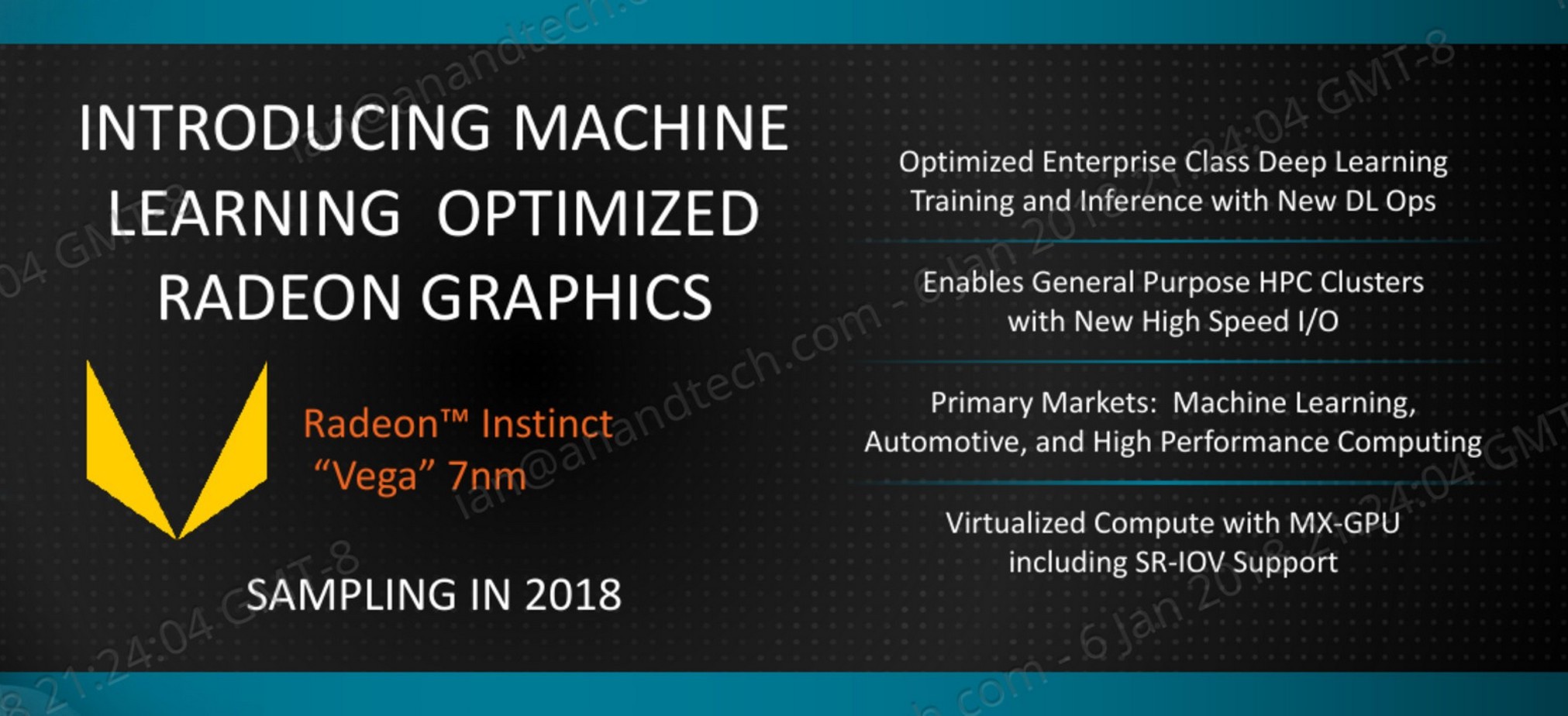
This slide above lays most of it out: the design will be an optimized version of Vega, which means it might not look much like a Vega GPU as we know it. AMD is planning that this product is used both for training and inference, with a focus on new deep learning operations – specifically aimed at HPC clusters. AMD also cites a new high-speed IO in play, which might be a version of Infinity Fabric designed to compete with NVLink, as well as virtualization support.
With 7nm in its infancy, we highly expect it to be a small bit of silicon, something akin to the current Radeon Instinct MI8. By using small silicon in a high margin market, this will allow AMD to optimize the design plans for its other 7nm products. This is what Ryan called a ‘pipe-cleaner’ processor, and it makes sense for semiconductor fabs to focus on smaller processors to start with, as these will yield at higher rates.
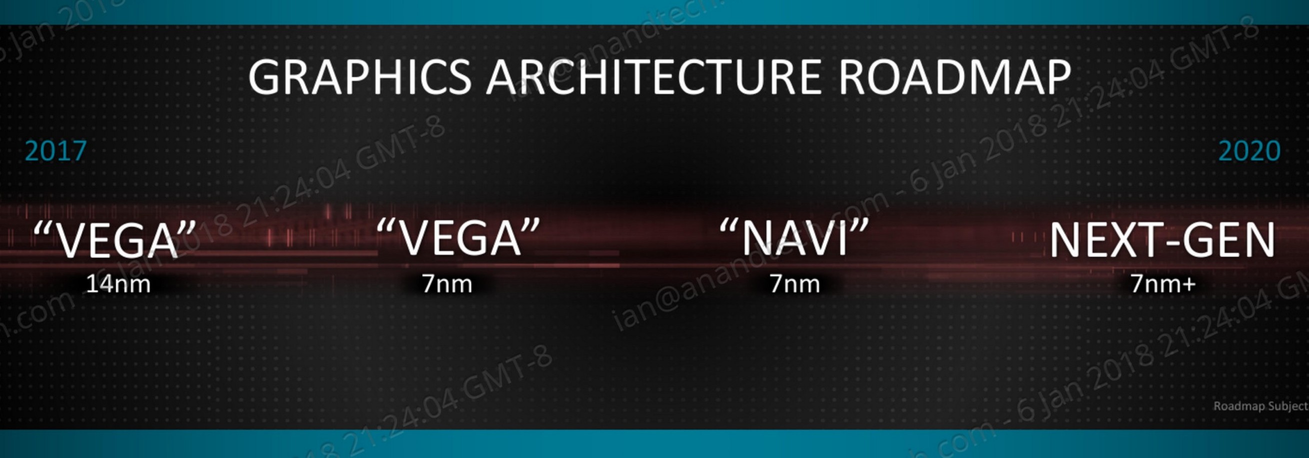
With a planned sampling in Q4 2018, we might expect volume production to be nearer Q2 2019. This means that the next generation of consumer-focused graphics, perhaps using the newer Navi architecture, will be in the mid-2019 timeframe. According to AMD’s roadmaps, it is committed to demonstrating Vega on 7nm, Navi on 7nm, and a ‘next-gen’ design on 7+ before the end of 2020. Obviously there was no clarification on whether that final design is consumer or enterprise focused for 2020. In our recent interview with AMD’s CEO, when asked if the GPU market will at some point have to bifurcate between gaming focused and compute focused designs, Dr. Lisa Su stated that ‘it must be the case’.
Updates on AMD and RTG
At the time of the event, AMD was in technical limbo, with former Radeon Technology Group leader Raja Koduri leaving for Intel. Since the event (i.e. between the event and the time this is published), AMD has reimagined the role and hired two people to fill it: Mike Rayfield will head up the business side of RTG, while David Yang, who used to work for AMD on GPUs, is rehired to take control of the technology side of RTG.
You can read our analysis of these hirings here.


131 Comments
View All Comments
mateau - Monday, January 8, 2018 - link
@Ian ..."It is our understanding that the 12nm process is essentially a 14+ process for GloFo"
Would you please a credible source for that statement. Say, EETimes or other such Industry outlet rather than an garnished from sites who do nothing other than plagiarize work that fits into the point they are try to make.
I too have read on-line media's dismissal of GloFo 12nm process. Everything that I have read on this matter is based upon an early on-line media piece highly critical to AMD that tried to minimize the impact of 12nm. GloFo on their website specifically states that 12nm is a NEW process node and it is 12nm. GloFo has announced that 12nm IS 12nm, a new shrink from 14nm. Announcing falsely would create all sorts of problems with the FTC and lawyers who do nothing but specialize in Class Action suits. Case in point Intel is getting it's clock cleaned due to their knowledge of and failure to eliminate the Meltdown hardware flaw.
As with ALL process nodes, the entire die is not fabbed with say 12nm or 14nm or for that matter the upcoming 7nm node. There are components within the die that can be and sometimes must be greater in size than the process node taped out for the silicon.
Perhaps you shaould also take the time to ask Dr. Su directly if ONE DESIGN covers ALL EPYC, RYZEN and Threadripper design? In my opinion EPYC is a design similar to Zeppelin and Ryzen but with some major design differences that make a server processor.
No sense speculating on something if you can ask AMD CEO directly.
A5 - Monday, January 8, 2018 - link
They may have been able to reduce the minimum possible feature size in a way that lets them claim a new number, but that doesn't necessarily mean that the performance of a finished product is significantly different.It's impossible to know until products are out in the world, because all we have for now is GloFo PR statements, which are going to make things look as rosy as possible.
SaturnusDK - Monday, January 8, 2018 - link
The Zeppelin die covers all Ryzen, Ryzen Pro, Threadripper, and EPYC CPUs. However, there are parts disabled on those designated Ryzen and Threadripper that are enabled on Ryzen Pro and EPYC. I do not know for certain if there is any feature differences between Ryzen Pro and EPYC but judging from AMDs own information there doesn't seem to be.Dr. Swag - Monday, January 8, 2018 - link
https://www.anandtech.com/show/11854/globalfoundri...based on improvements in the 10-20% range calling it "essentially a 14nm+ node" seems reasonable to me.
iwod - Monday, January 8, 2018 - link
Huh?Meltdown - Not relevant here.
TSMC called their 16nm++ ( or was it 16nm +++ ) as 12nm.
And FTC would have a problem with Intel because their 10nm really should be 7nm by Fab Industry measurement.
And it is not garish, it is straight from GF investor conference.
Design? Speculate? Is Goldmount the same design as Goldmount+. Do QA and feature / yield test accounts for design? And more importantly, do even any other chip maker disclose these information? There is something call trade secret.
LurkingSince97 - Thursday, January 18, 2018 - link
It is well known knowledge that GloFlo 're-branded' their 14nm+ to 12nm.There is nearly a dozen different feature sizes in a process these days, no one number captures it.
Also, GloFlo is not the only one that has done this sort of thing.
LurkingSince97 - Thursday, January 18, 2018 - link
To be more specific, GloFo's own conference / announcement talked about the name change... AMD's roadmaps had "Zen+" on a GloFo 14nm+ node, then suddenly that same roadmap changed it to "12nm" when GloFo announced the new node (and named it)coolhardware - Monday, January 8, 2018 - link
Get well soon Ian!Luposian - Wednesday, January 10, 2018 - link
Wouldn't now be a perfect time to implement changes to the predictive branch execution portions of the new processors, to eliminate issues with Spectre and Meltdown, since they're just making these processors now?LurkingSince97 - Thursday, January 18, 2018 - link
They have _finished_ the Zen 2 design. Zen already doesn't have problems with Meltdown. Spectre is a lot harder to do anything about, other than maybe adding an instruction for a branch prediction barrier. Maybe they had time to add that to Zen 2, or maybe it can be done even in Zen+ without much trouble. Your software will need to be recompiled against it, however.