AMD Tech Day at CES: 2018 Roadmap Revealed, with Ryzen APUs, Zen+ on 12nm, Vega on 7nm
by Ian Cutress on February 1, 2018 8:45 AM EST2nd Generation Ryzen
AMD has always stated that its Zen core design will form the basis of its high-performance x86 processors for the foreseeable future. This has included, among other things, a cadence with releasing updates and new Zen-like processor designs into the market. As announced at Tech Day, the update to 1st Generation Ryzen will be 2nd Generation Ryzen, coming in April 2018.
Specific core counts, frequencies, or model numbers were not mentioned – we are still 2-3 months away from this launch. AMD did state a number of points worth discussing however, especially with its decision to use GlobalFoundries newest 12nm ‘LP’ design process (12LP), compared to the 14nm ‘LPP’ design process (14LPP) used in the first generation Ryzen products.
First I want to go to this graph, to show what AMD want to claim on raw performance over the next three years:
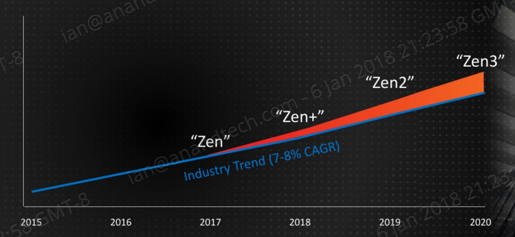
This is a graph of raw performance, combining both the efficiency of processing instructions (IPC, instructions per clock) as well as benefits from an improved manufacturing process. AMD cites the industry trend as growing 7-8% every year, and that they fully expect the Zen package, due to design improvements in the microarchitecture and better foundry notes, will go above and beyond that 7-8% figure.
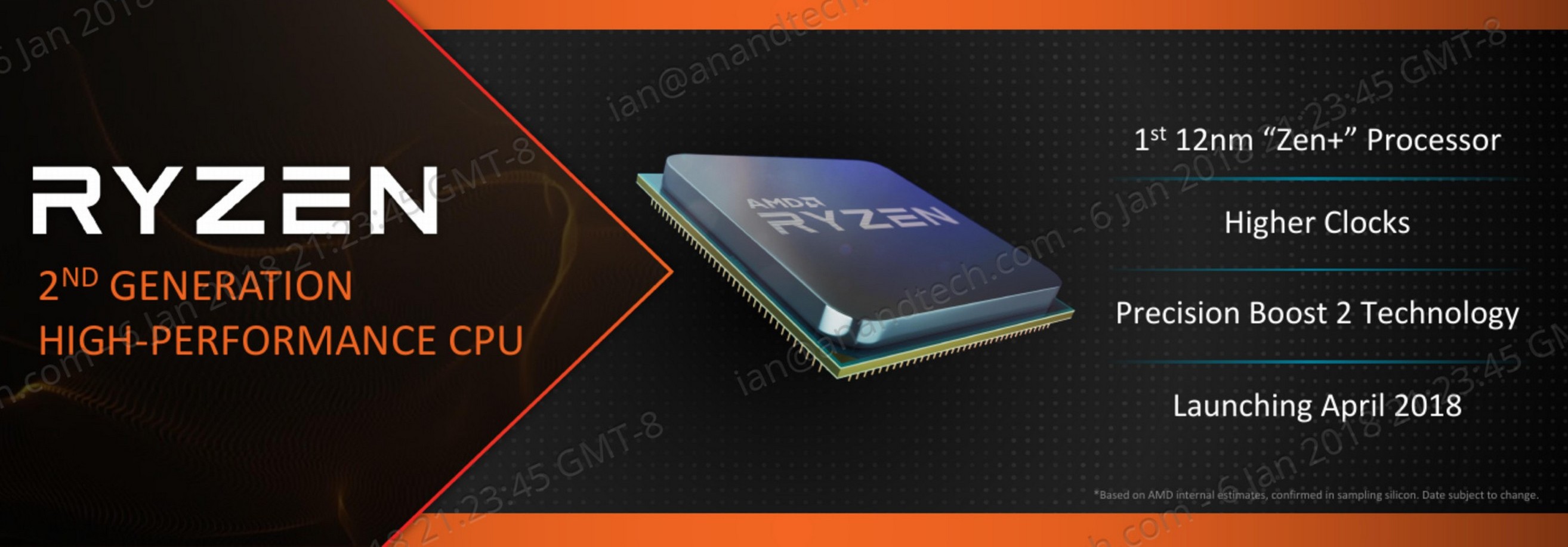
So first up along that line is Zen+. This will be the name of the core in the 2nd Generation Ryzen family, built on GlobalFoundries 12LP process. AMD has categorically stated that the core microarchitecture underneath has not changed: we will still have the same front-end and back-end as Zen, with the same size caches and the same layout. What has changed will be some of the power management algorithms, and perhaps some tweaks to the neural network-based prefetch algorithms. This will be headlined as ‘Precision Boost 2’ support, which is a feature that has already been introduced to the Ryzen with Vega graphics components (desktop and mobile).
GlobalFoundries 12LP
Most of the physical changes happen due to the process. Last year, AMD cited that its second generation Ryzen products will be on a ‘14+’ manufacturing node, but now it is going to be on a 12LP process. Some people argue that this is a clever marketing ploy as a name change, given nothing in the designs actually comes close to 14nm or 12nm. We were told that 12LP implements stricter design rules for the manufacturing process, requiring changes to library layout and the floorplan, but with an end result of a focus on performance per watt.
For the new processors, AMD is claiming a 10% boost in performance per watt overall. This is going to be taken as higher clocks for the same power at the high-end and lower power for the same frequency for more power sensitive products. AMD’s slide from Jim Anderson’s presentation above specifically says ‘higher clocks’, which when combined with Mark Papermaster’s presentation which states ‘10%+ performance vs. 14LPP’, we could take this to mean that we should expect anywhere from an 8%+ increase in frequencies with 2nd Generation Ryzen for desktop (not 10%, accounting for the fact that the power/efficiency curve gets worse the faster you are).
| Comparison of 14 nm Branded Process Technologies | |||||||
| GlobalFoundries 12LP |
GlobalFoundries 14HP |
GlobalFoundries 14LPP ? |
TSMC 16FF |
Intel 14nm |
|||
| Fin Pitch | ? | ? | ? | ? | 42 nm | ||
| Gate Pitch | ? | ? | 78 nm | 90 nm | 70 nm | ||
| Min Metal Pitch | ? | ? | 64 nm | 64 nm | 52 nm | ||
| Gate Height | ? | ? | less than 480 nm | 480 nm | 399 nm | ||
| Metal Layers | 13 | 17 | 13 | unknown | unknown | ||
| Design Library | 7.5T | 12T | 9T | 9T | unknown | ||
The 10% figure is corroborated by GlobalFoundries, who back in 2017 stated that its 12LP process will offer a 10% better performance. GF also stated that the 12LP process also offers a 15% area reduction against 14LPP. This is done, according to GlobalFoundries, by using 7.5T libraries rather than 9T libraries. This requires its customers to ‘recompile’ their 14LPP designs for the adjusted 12LP process.
To put this into context, this means we might see 4.3-4.5 GHz processors with the 2nd Generation Ryzen sticker where we used to see 4.0 GHz processors. It will be interesting to see how AMD and GlobalFoundries have moved that seemingly hard overclock limit we saw on processors like the Ryzen 7 1800X, which had a hard time moving past 4.2 GHz on all cores.
We are having a tour around GlobalFoundries Fab 8 in New York this week, and are set to spend some time with CTO Gary Patton, talking about the new process. While he is unlikely to quote specifically about how AMD has used the new design rules to its advantage, he might tell us some more information about the process in general.
As for 2nd Generation Ryzen, we are told that the major motherboard vendors and OEMs already have near-final engineering samples to hand to ensure updated compatibility.
New Motherboards: X470 Chipset and AM4 Motherboards
Launching around the same time as the new processors will be a range of X470 motherboards from the main motherboard manufacturers. Strictly speaking, these motherboards are not needed: the current AM4 motherboards based on the X370/B350/A320 chipsets on the market will accept the new processors (as well as APUs) with a relevant BIOS update. However, AMD plans to optimize its high-end chipset with a few new features.
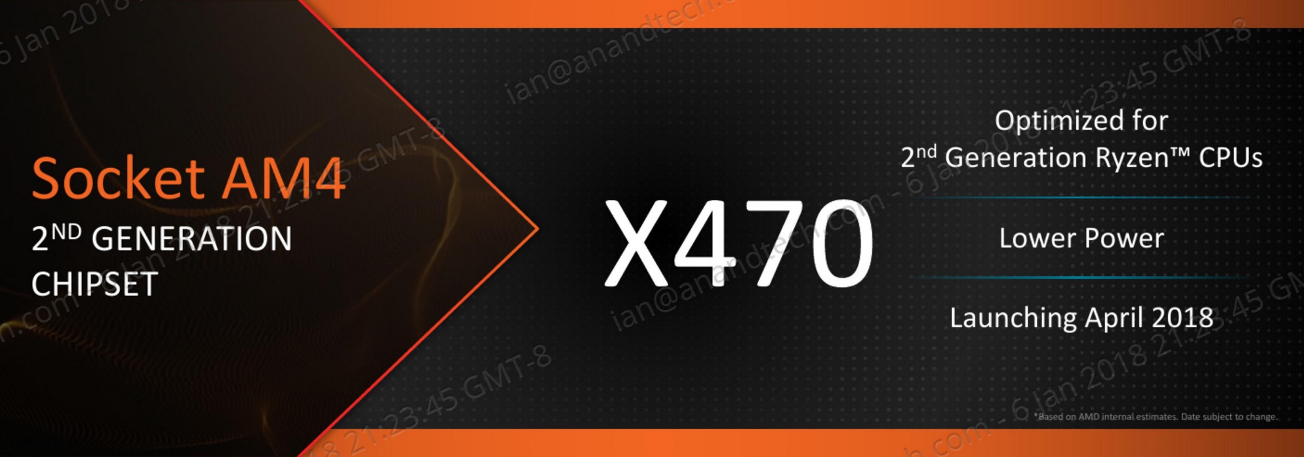
What we know so far is that the new X470 chipset is designed for lower power. How that is achieved, AMD would not go into at this point, however the fact that the X370 chipset was an outsourced product through ASMedia built on TSMC’s 55nm process would point to at least one way AMD could save power: building it on TSMC’s 40nm process for a start. We are told that the X370 and X470 chipsets are pin-compatible, which is not a limit to this theory, but an interesting point nonetheless.
AMD has stated that the new chipsets will be optimized better for the newer processors, which can be translated as better memory support and a few newer features. We were told that X470 will have very specific new features, although AMD did not want to disclose anything until we get closer to the launch.
We were lucky enough to see a GIGABYTE based X470 motherboard at CES.
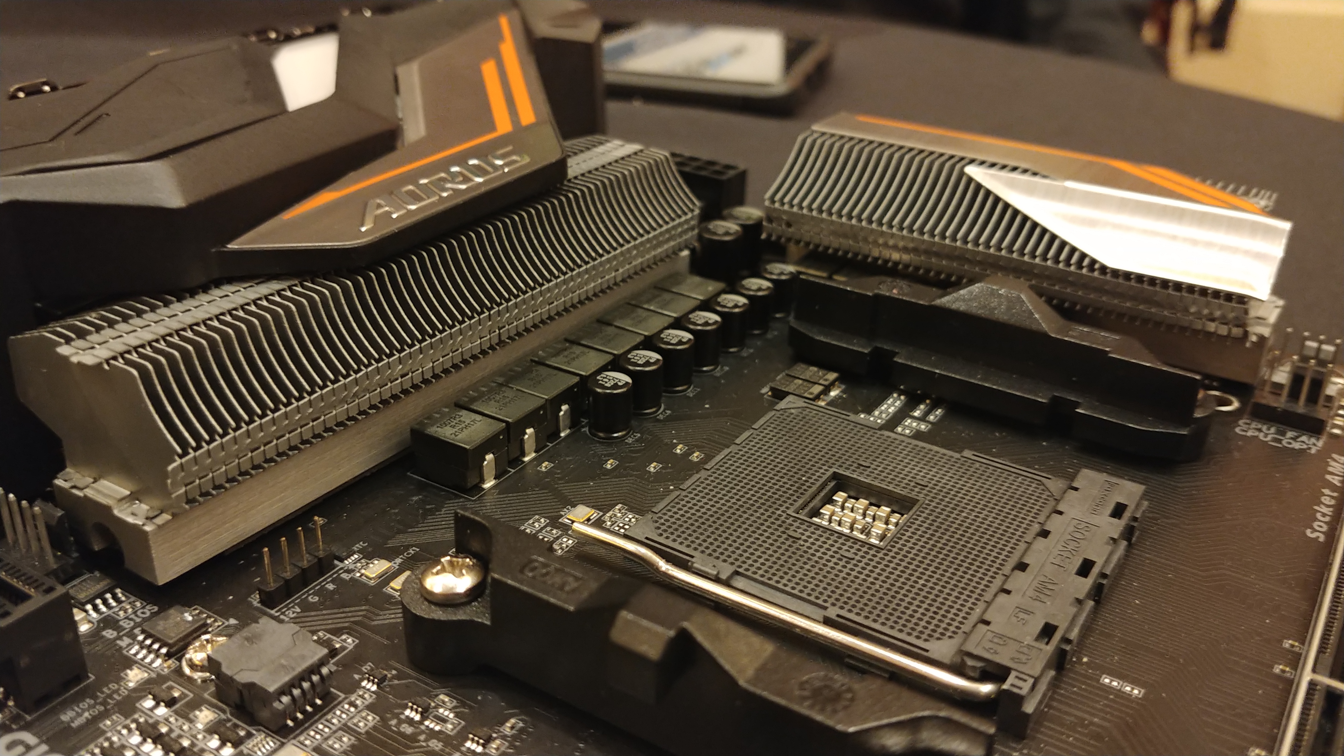
You can read our analysis on this motherboard here.
Second Generation Threadripper
In the second half of 2018, AMD will launch a second generation of Threadripper, based on the new 12LP process. AMD did not go into specific details here, mainly because the launch is so far away, but users should look forward to the same improvements as the standard Ryzen products: up to 10% better raw performance due to the improved manufacturing process, Precision Boost 2 support, and better memory compatibility.
We are not expecting anything to change on core counts or other features like PCIe lanes.


131 Comments
View All Comments
mateau - Monday, January 8, 2018 - link
@Ian ..."It is our understanding that the 12nm process is essentially a 14+ process for GloFo"
Would you please a credible source for that statement. Say, EETimes or other such Industry outlet rather than an garnished from sites who do nothing other than plagiarize work that fits into the point they are try to make.
I too have read on-line media's dismissal of GloFo 12nm process. Everything that I have read on this matter is based upon an early on-line media piece highly critical to AMD that tried to minimize the impact of 12nm. GloFo on their website specifically states that 12nm is a NEW process node and it is 12nm. GloFo has announced that 12nm IS 12nm, a new shrink from 14nm. Announcing falsely would create all sorts of problems with the FTC and lawyers who do nothing but specialize in Class Action suits. Case in point Intel is getting it's clock cleaned due to their knowledge of and failure to eliminate the Meltdown hardware flaw.
As with ALL process nodes, the entire die is not fabbed with say 12nm or 14nm or for that matter the upcoming 7nm node. There are components within the die that can be and sometimes must be greater in size than the process node taped out for the silicon.
Perhaps you shaould also take the time to ask Dr. Su directly if ONE DESIGN covers ALL EPYC, RYZEN and Threadripper design? In my opinion EPYC is a design similar to Zeppelin and Ryzen but with some major design differences that make a server processor.
No sense speculating on something if you can ask AMD CEO directly.
A5 - Monday, January 8, 2018 - link
They may have been able to reduce the minimum possible feature size in a way that lets them claim a new number, but that doesn't necessarily mean that the performance of a finished product is significantly different.It's impossible to know until products are out in the world, because all we have for now is GloFo PR statements, which are going to make things look as rosy as possible.
SaturnusDK - Monday, January 8, 2018 - link
The Zeppelin die covers all Ryzen, Ryzen Pro, Threadripper, and EPYC CPUs. However, there are parts disabled on those designated Ryzen and Threadripper that are enabled on Ryzen Pro and EPYC. I do not know for certain if there is any feature differences between Ryzen Pro and EPYC but judging from AMDs own information there doesn't seem to be.Dr. Swag - Monday, January 8, 2018 - link
https://www.anandtech.com/show/11854/globalfoundri...based on improvements in the 10-20% range calling it "essentially a 14nm+ node" seems reasonable to me.
iwod - Monday, January 8, 2018 - link
Huh?Meltdown - Not relevant here.
TSMC called their 16nm++ ( or was it 16nm +++ ) as 12nm.
And FTC would have a problem with Intel because their 10nm really should be 7nm by Fab Industry measurement.
And it is not garish, it is straight from GF investor conference.
Design? Speculate? Is Goldmount the same design as Goldmount+. Do QA and feature / yield test accounts for design? And more importantly, do even any other chip maker disclose these information? There is something call trade secret.
LurkingSince97 - Thursday, January 18, 2018 - link
It is well known knowledge that GloFlo 're-branded' their 14nm+ to 12nm.There is nearly a dozen different feature sizes in a process these days, no one number captures it.
Also, GloFlo is not the only one that has done this sort of thing.
LurkingSince97 - Thursday, January 18, 2018 - link
To be more specific, GloFo's own conference / announcement talked about the name change... AMD's roadmaps had "Zen+" on a GloFo 14nm+ node, then suddenly that same roadmap changed it to "12nm" when GloFo announced the new node (and named it)coolhardware - Monday, January 8, 2018 - link
Get well soon Ian!Luposian - Wednesday, January 10, 2018 - link
Wouldn't now be a perfect time to implement changes to the predictive branch execution portions of the new processors, to eliminate issues with Spectre and Meltdown, since they're just making these processors now?LurkingSince97 - Thursday, January 18, 2018 - link
They have _finished_ the Zen 2 design. Zen already doesn't have problems with Meltdown. Spectre is a lot harder to do anything about, other than maybe adding an instruction for a branch prediction barrier. Maybe they had time to add that to Zen 2, or maybe it can be done even in Zen+ without much trouble. Your software will need to be recompiled against it, however.