AMD Tech Day at CES: 2018 Roadmap Revealed, with Ryzen APUs, Zen+ on 12nm, Vega on 7nm
by Ian Cutress on February 1, 2018 8:45 AM ESTZen and Vega: Ryzen PRO Mobile
In the second half of last year, AMD’s Enterprise, Embedded and Semi-Custom division (now the Enterprise and Embedded division) launched its Ryzen PRO family of desktop processors, for business customers that needed additional management capabilities. AMD has been making ‘Pro’ versions of its consumer processors for several generations now, usually mimicking the specifications of the consumer products aside from the management support.
These products, by and large, go up against Intel’s equivalent vPro processors, and AMD’s value add revolves around support for DASH, an open-source management protocol, TSME (transparent secure memory encryption), and its commitment to customer requests such as operating system image stability (18-months), guaranteed processor availability (24-months), manufacturing specifications designed for long-term reliability, and a commercial limited warranty (36-months). AMD also likes to tout that it offers a Pro product at the lower end of the market, where Intel does not have a vPro-enabled Core i3.
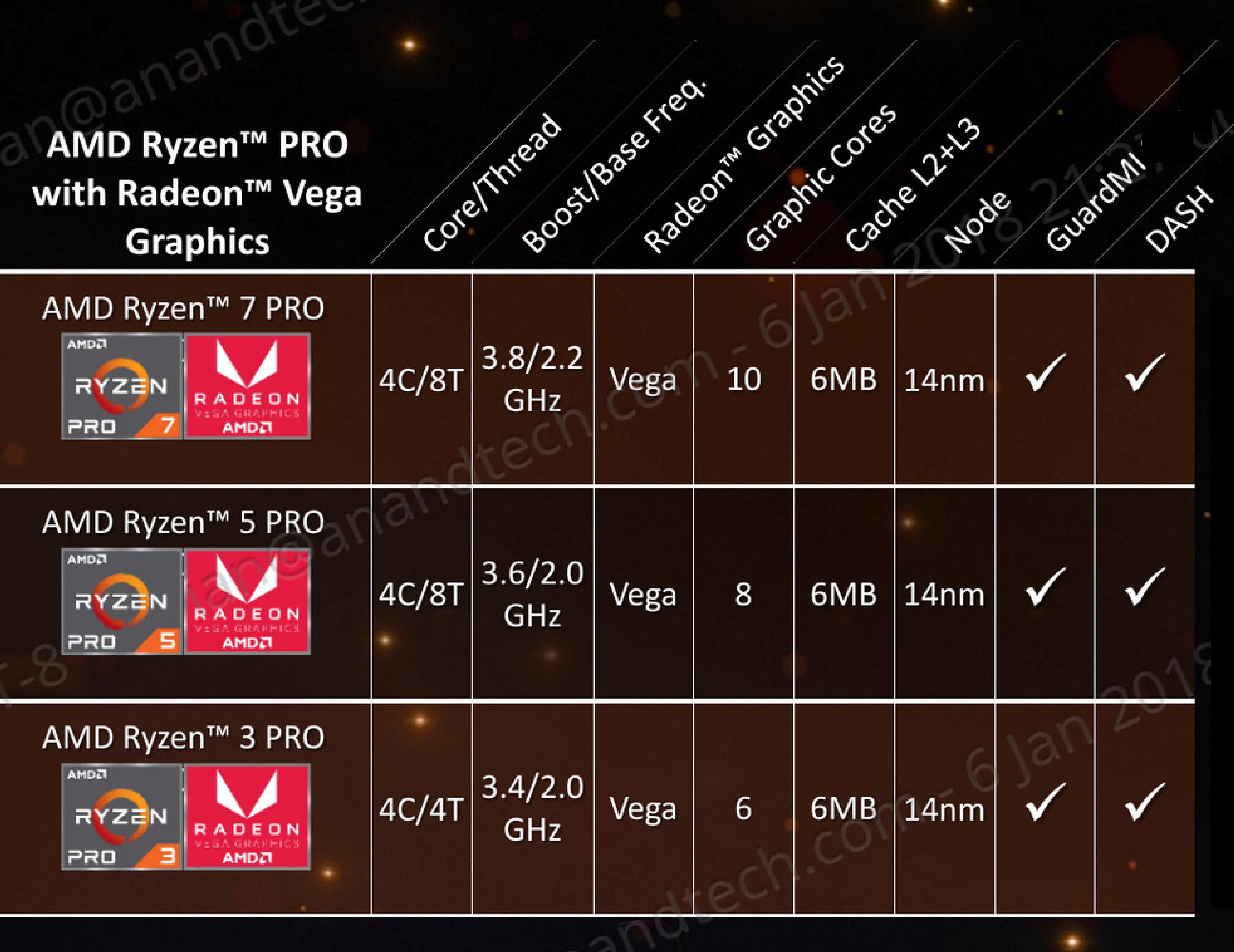
As part of the AMD Tech Day, it was announced that the Ryzen PRO Mobile family will be launched in Spring 2018. These components are, by and large, the Ryzen Mobile family of processors with Vega graphics but with the added Pro features listed above. For performance and power, AMD states similar sorts of numbers as it did with the launch of Ryzen Mobile: up to 270% better performance per watt, targeting 13 hours of useful battery life, 9 hours of HD video playback, and targeting a generation of sleek and powerful laptops, in this case focused for the Enterprise market.
So much like the Ryzen 7 2700U, the Ryzen 5 2500U, and the Ryzen 3 2300U, AMD will launch the Ryzen PRO Mobile equivalents:
We are likely to see OEMs that currently provide AMD A-Series PRO notebooks to offer updated versions with these new processors, as well as a series of new designs coming into the business and enterprise market.


131 Comments
View All Comments
mateau - Monday, January 8, 2018 - link
@Ian ..."It is our understanding that the 12nm process is essentially a 14+ process for GloFo"
Would you please a credible source for that statement. Say, EETimes or other such Industry outlet rather than an garnished from sites who do nothing other than plagiarize work that fits into the point they are try to make.
I too have read on-line media's dismissal of GloFo 12nm process. Everything that I have read on this matter is based upon an early on-line media piece highly critical to AMD that tried to minimize the impact of 12nm. GloFo on their website specifically states that 12nm is a NEW process node and it is 12nm. GloFo has announced that 12nm IS 12nm, a new shrink from 14nm. Announcing falsely would create all sorts of problems with the FTC and lawyers who do nothing but specialize in Class Action suits. Case in point Intel is getting it's clock cleaned due to their knowledge of and failure to eliminate the Meltdown hardware flaw.
As with ALL process nodes, the entire die is not fabbed with say 12nm or 14nm or for that matter the upcoming 7nm node. There are components within the die that can be and sometimes must be greater in size than the process node taped out for the silicon.
Perhaps you shaould also take the time to ask Dr. Su directly if ONE DESIGN covers ALL EPYC, RYZEN and Threadripper design? In my opinion EPYC is a design similar to Zeppelin and Ryzen but with some major design differences that make a server processor.
No sense speculating on something if you can ask AMD CEO directly.
A5 - Monday, January 8, 2018 - link
They may have been able to reduce the minimum possible feature size in a way that lets them claim a new number, but that doesn't necessarily mean that the performance of a finished product is significantly different.It's impossible to know until products are out in the world, because all we have for now is GloFo PR statements, which are going to make things look as rosy as possible.
SaturnusDK - Monday, January 8, 2018 - link
The Zeppelin die covers all Ryzen, Ryzen Pro, Threadripper, and EPYC CPUs. However, there are parts disabled on those designated Ryzen and Threadripper that are enabled on Ryzen Pro and EPYC. I do not know for certain if there is any feature differences between Ryzen Pro and EPYC but judging from AMDs own information there doesn't seem to be.Dr. Swag - Monday, January 8, 2018 - link
https://www.anandtech.com/show/11854/globalfoundri...based on improvements in the 10-20% range calling it "essentially a 14nm+ node" seems reasonable to me.
iwod - Monday, January 8, 2018 - link
Huh?Meltdown - Not relevant here.
TSMC called their 16nm++ ( or was it 16nm +++ ) as 12nm.
And FTC would have a problem with Intel because their 10nm really should be 7nm by Fab Industry measurement.
And it is not garish, it is straight from GF investor conference.
Design? Speculate? Is Goldmount the same design as Goldmount+. Do QA and feature / yield test accounts for design? And more importantly, do even any other chip maker disclose these information? There is something call trade secret.
LurkingSince97 - Thursday, January 18, 2018 - link
It is well known knowledge that GloFlo 're-branded' their 14nm+ to 12nm.There is nearly a dozen different feature sizes in a process these days, no one number captures it.
Also, GloFlo is not the only one that has done this sort of thing.
LurkingSince97 - Thursday, January 18, 2018 - link
To be more specific, GloFo's own conference / announcement talked about the name change... AMD's roadmaps had "Zen+" on a GloFo 14nm+ node, then suddenly that same roadmap changed it to "12nm" when GloFo announced the new node (and named it)coolhardware - Monday, January 8, 2018 - link
Get well soon Ian!Luposian - Wednesday, January 10, 2018 - link
Wouldn't now be a perfect time to implement changes to the predictive branch execution portions of the new processors, to eliminate issues with Spectre and Meltdown, since they're just making these processors now?LurkingSince97 - Thursday, January 18, 2018 - link
They have _finished_ the Zen 2 design. Zen already doesn't have problems with Meltdown. Spectre is a lot harder to do anything about, other than maybe adding an instruction for a branch prediction barrier. Maybe they had time to add that to Zen 2, or maybe it can be done even in Zen+ without much trouble. Your software will need to be recompiled against it, however.