Intel Core with Radeon RX Vega M Graphics Launched: HP, Dell, and Intel NUC
by Ian Cutress on January 7, 2018 9:02 PM EST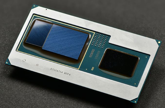
It’s here – one of the most unlikely partnerships in the semiconductor industry. Long-time rivals Intel and AMD, battling out of x86 dominance for over 35 years, are now co-conspirators. Take one part Intel’s high-performance 8th generation processor core, one part with AMD’s efficient Vega graphics, mix together with 4 GB of HBM memory and sprinkle in some high-performance interconnect.
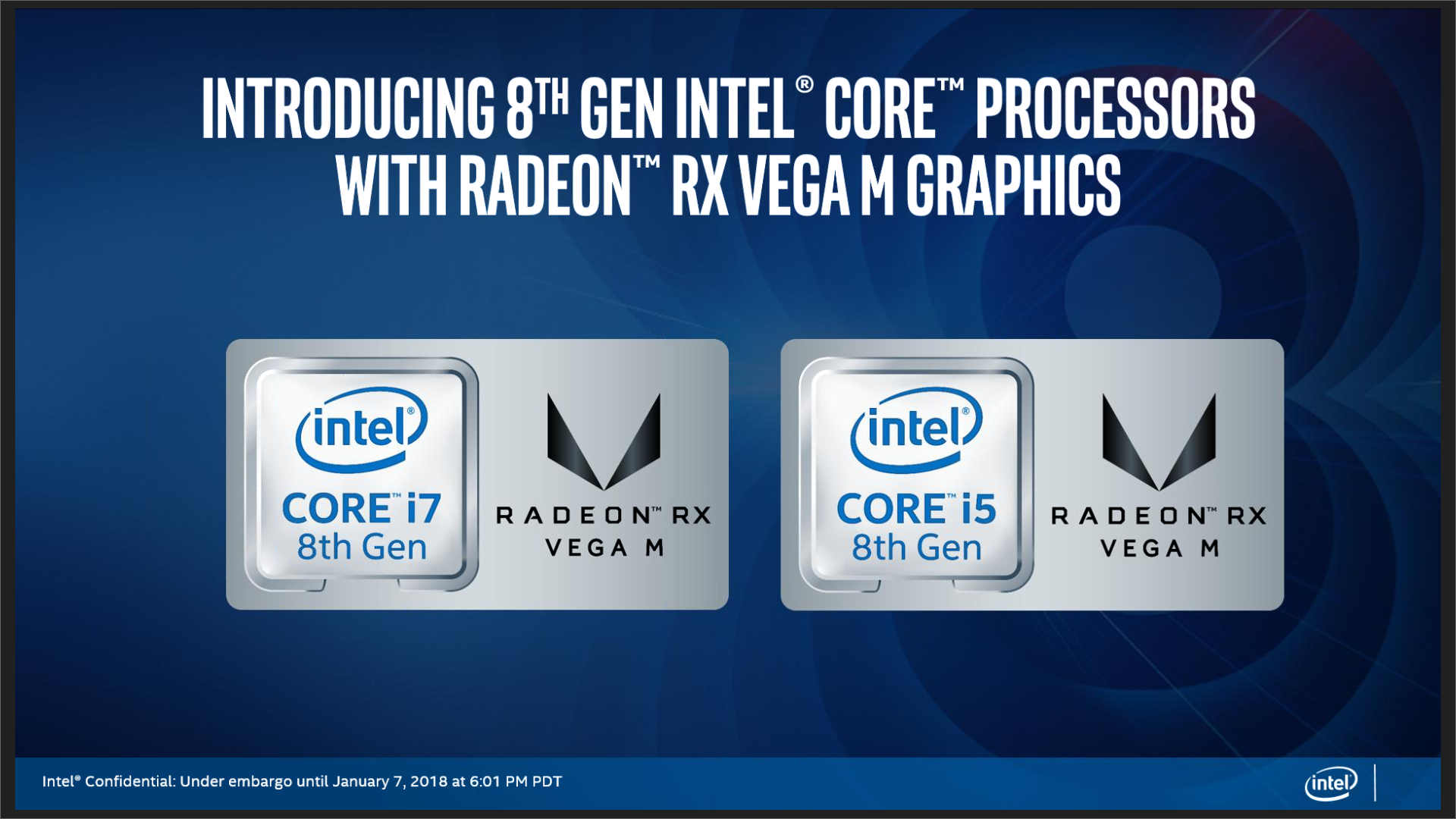
The new products are officially labeled as ‘Intel 8th Generation Core with Radeon RX Vega M Graphics’, although this will be shortened to ‘Intel with Radeon Graphics’ for ease of use.
Intel with Radeon Graphics is strictly speaking a new Intel specific product, to be marketed and distributed as such. Today’s official launch builds on the platform announcement made late last year, with added additional specifications, confirmation of the feature set, and a series of new products based on Intel with Radeon Graphics are set to be announced this week at CES from Dell, HP, and Intel's own NUC. Aside from the NUC, we've been told to hold the other vendor information until their embargo times have arrived.
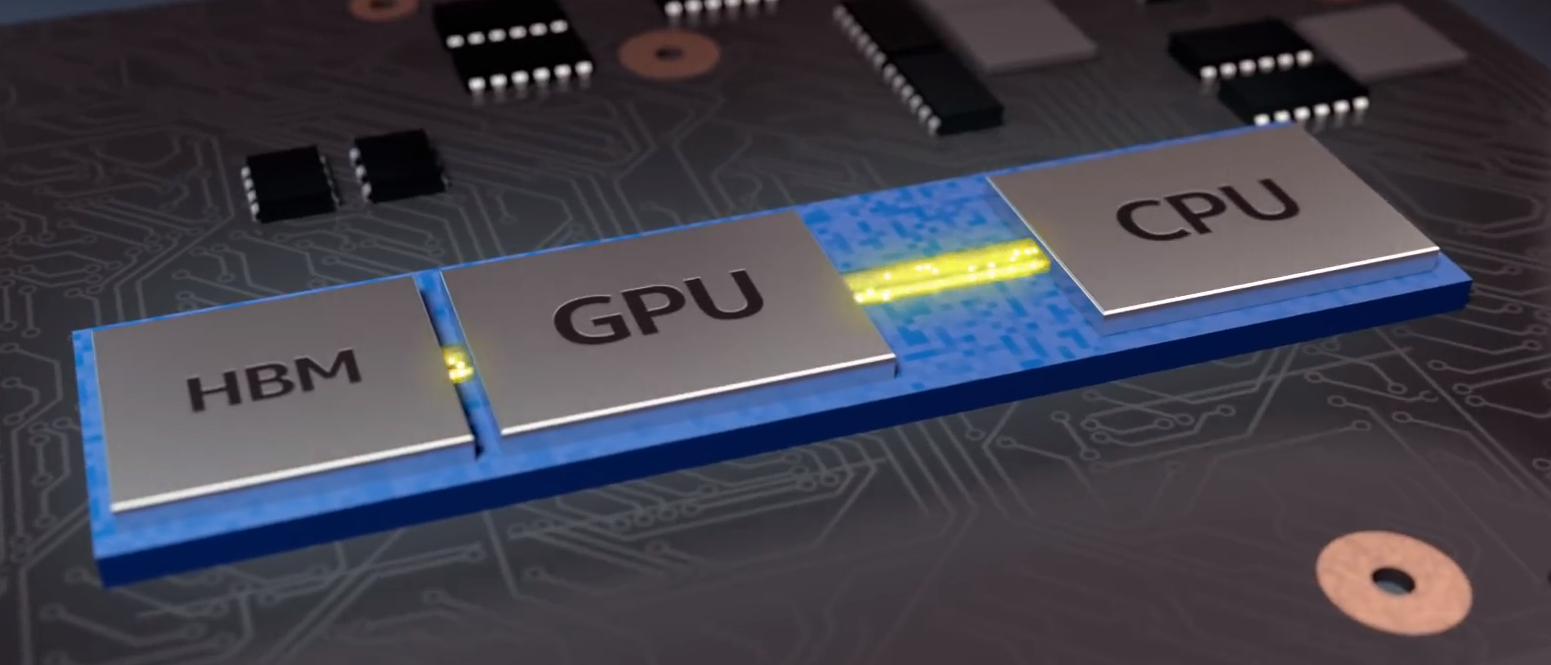
As we explained in our previous coverage, Intel with Radeon Graphics uses an ‘H-series’ Intel central processor and an AMD Radeon graphics processor as two distinct bits of silicon on the same package (a multi-chip package). Intel is buying the graphics processor from AMD, much like any other silicon purchase, and as a result, AMD’s involvement is strictly business. The graphics processor part is designed by AMD’s semi-custom division that deals with custom designs, such as the chips that go into Sony’s PlayStation 4 and Microsoft’s Xbox line. The graphics is connected to high-bandwidth memory, specifically the second generation HBM (known as HBM2), and the connection between the two uses Intel’s new embedded multi-die interconnect bridge technology, or EMIB for short. In other words, Intel CPU + AMD GPU + HBM2 + EMIB – acronyms are ablaze with these new chips.
The new products are an expansion of Intel’s traditional mobile product segmentation, which up until this point has been known as ‘YUH’. The new products fall under the ‘G’ name, designed to combine the high-performance of a H processor with the versatility of a U processor. The overall list of five/six segments, including the desktop and extreme segments, now looks as follows:
- Y – SoCs up to 4.5W, for portable fanless designs and 2-in-1s
- U – SoCs around 15W, for sleek high-performance lifestyle products
- H – CPUs around 35W/45W, offering more cores for larger enthusiast notebooks
- G – CPUs with additional graphics*, up to 100W
- S – Desktop processors
- X – A special segment for high-end desktops based on server processors
*May or may not have a separate graphics chip
The G-class Intel with Radeon Graphics processors being launched today are bigger than the standard processors that we would normally expect for mobile platforms, coming in with a TDP of 65W and 100W, although how power is managed between the two is part of Intel’s story with the new processors.
Without further ado, the specifications for the new parts are as follows:
| Intel's 8th Generation Core Processors with Radeon RX Vega M Graphics |
|||||
| Core i7-8809G |
Core i7-8709G |
Core i7-8706G |
Core i7-8705G |
Core i5-8305G |
|
| CPU uArch | Kaby Lake | Kaby Lake | |||
| On-Package Graphics (pGPU) |
Radeon RX Vega M GH | Radeon RX Vega M GL | |||
| CPU Cores | 4 / 8 | 4 / 8 | |||
| CPU Base Freq | 3.1 GHz | 3.1 GHz | 3.1 GHz | 3.1 GHz | 2.8 GHz |
| CPU Turbo Freq | 4.2 GHz | 4.1 GHz | 4.1 GHz | 4.1 GHz | 3.8 GHz |
| pGPU Compute Units | 24 CUs (1536 SPs) | 20 CUs (1280 SPs) | |||
| pGPU Frequency | 1063 MHz (1190 MHz Boost) |
931 MHz (1101 MHz Boost) |
|||
| pGPU Pixels/Clock | 64 | 32 | |||
| CPU PCIe Lanes | 8 to Radeon Graphics 8 for Other Use |
8 to Radeon Graphics 8 for Other Use |
|||
| Chipset + PCIe | 200-series derivative? 14-20 PCIe 3.0 Lanes |
200-series derivative? 14-20 PCIe 3.0 Lanes |
|||
| Package TDP | 100 W | 65 W | |||
| HBM2 Capacity | 4 GB | 4 GB | |||
| HBM2 Frequency | 800 MHz | 700 MHz | |||
| HBM2 Bit-Width | 1024-bit | 1024-bit | |||
| HBM2 Bandwidth | 204.8 GB/s | 179.2 GB/s | |||
| Quoted SP Perf | Up to 3.7 TFLOPS (SP) | Up to 2.6 TFLOPS (SP) | |||
| Intel HD Graphics | HD 630 | HD 630 | |||
| iGPU Frequency | Up to 1100 MHz | Up to 1100 MHz | |||
| DRAM | Dual Channel, DDR4-2400 | Dual Channel, DDR4-2400 | |||
| ECC | No | No | |||
| vPro | No | No | Yes | No | No |
| Overclocking | CPU, iGPU, pGPU, HBM | No | No | No | No |
*Added Core i7-8706G on 1/8
Each of the new parts is a quad-core design using HyperThreading, with Intel’s HD 630 GT2 graphics as the traditional ‘integrated’ low power graphics (iGPU) for video playback and QuickSync. This is connected via eight PCIe 3.0 lanes to the ‘package’ graphics (pGPU) chip, the Radeon RX Vega M, leaving 8 PCIe 3.0 lanes from the CPU to use for other functionality (GPU, FPGA, RAID controller, Thunderbolt 3, 10 Gigabit Ethernet).
On the Radeon RX Vega M graphics, there is one version of the silicon for which there will be two variants: the ‘GH’ will be the highest part (H for high) with 24 compute units (1536 streaming processors), 64 pixels per clock, running at a base frequency of 1063 MHz and can boost up to 1190 MHz. The second variant is the GL part (L for low), with 20 compute units (1280 streaming processors), 32 pixels per clock, running at a base frequency of 931 MHz and can boost up to 1011 MHz.
Both pGPU Radeon variants will have access to 4GB of HBM2 as an immediate graphics memory (this is not available to the CPU as DRAM). With one stack of HBM2, this means a 1024-bit bus width, which for the GH parts runs at 800 MHz for 208.6 GB/s bandwidth, or for the GL parts runs at 700 MHz for 179.6 GB/s bandwidth. Intel likes to stress that this bandwidth is only possible due to its EMIB technology, as currently all non-Intel HBM2 products available require an expensive bulky interposer that adds z-height: by using EMIB, Intel claims, the performance is on par with an interposer without the added bulk or most of the cost.
Only the Core i7-8809G, the highest placed processor, will offer overclocking. Intel has defined this chip as able to overclock the processor core, the integrated graphics frequency, the package graphics frequency, and the high bandwidth memory frequency (as well as system level DRAM). Overclocking will be dependent on how the vendor implements the feature set and software: nominally Intel is stating that in Windows 10, the CPU/iGPU can be overclocked through Intel XTU software, while the pGPU and HBM2 will need AMD’s Radeon Wattman software. It is not clear if/when an Intel-specific version of the latter will be distributed, given that when asked where the driver/software stack for the Radeon graphics should come from, we were told ‘all the software will come from Intel, consider this a fully-enabled Intel processor’.
We confirmed with Intel that all the processors support VT-x and VT-d, and that none of the processors support ECC. Only the i7-8706G is vPro enabled.


66 Comments
View All Comments
skavi - Monday, January 8, 2018 - link
Do we even have 8th gen Y?evilpaul666 - Sunday, January 7, 2018 - link
So is this all Intel has for CES?extide - Sunday, January 7, 2018 - link
So, here we have a MCM with chips from three different fabs on it. 1 from Intel, 1 from GF, and one from Samsung or SKHynix.Have we ever seen something like that before?
Penti - Sunday, January 7, 2018 - link
So will we see a 24 CU Vega-chip with HBM2 as a discrete chip for laptops too? It's essentially designed as a lower tier RTG/AMD GPU, kinda specced like a replacement for Polaris 11.Cooe - Monday, January 8, 2018 - link
AMD announced Vega Mobile today which is pretty much exactly that. It's a freaking tiny package,and for that reason I expect it to be pretty successful vs Nvidia's traditional GDDR5 designs. (Though no word yet if the Vega Mobile and the semi-custom chip here are the same as far as CU count and what not, but it wouldn't be surprising).
Penti - Monday, January 8, 2018 - link
Same Z-height as KBL-G at least. Vega mobile was expected, is definitively related to the chip on the KBL-G package but might be a chip with a slightly different CU/SP count but renders make it look exactly the same.flashbacck - Sunday, January 7, 2018 - link
"Intel’s internal graphics, known as ‘Gen’ graphics externally, has been third best behind NVIDIA and AMD for grunt."Grunt? huh?
Holliday75 - Monday, January 8, 2018 - link
I thought the same thing.Kevin G - Sunday, January 7, 2018 - link
The one thing missing from this article, which I think if fair in the context of the fury of news last week, are Spectre and Meltdown. Intel is currently facing multiple law suits about it, especially in the context of bringing to market with a security flaw. These security flaws maybe the death blow to Cannon Lake which was originally to be a late 2018 part and already had the desktop parts removed form the line up in favor of Coffee Lake.There is another Lake part coming in late 2018 called Whiskey Lake and the rumors are pointing toward it being yet another Sky Lake based 14 nm part (see Kaby and Coffee Lake). I have no idea what these parts could provide other than potential fixes for Meltdown and Spectre minus the offhand possibility of an updated GPU. Next actual CPU core design is set to be Ice Lake which may also be their first 10 nm chip. Intel has shied away from doing to many firsts as once due to the difficulty of isolating problem (is it process? design? packaging? interconnect?) but Intel may have no choice.
Intel's CEO is set to take the stage at CES tomorrow so we'll probably get some answers to their roadmap as well has some groveling about Meltdown and Spectre.
Oh, for the curious, you can look up what codenames Intel does have the horizon here and see Whiskey Lake for yourselves:
https://www.intel.com/content/www/us/en/design/pro...
UtilityMax - Thursday, January 11, 2018 - link
This gotta be the worst time to announce a new Intel CPU. Sadly, I think the sheep that are the average consumers will gladly buy PCs with these CPUs.