HiSilicon Kirin 970 - Android SoC Power & Performance Overview
by Andrei Frumusanu on January 22, 2018 9:15 AM ESTAn Introduction to Neural Network Processing
AI is currently the big buzzword when talking about consumer electronics. While marketing departments all over are trying to embrace the term, when we’re talking about the current use of AI in computing terms we’re specifically talking about machine learning. More precisely when talking about the latest generations of silicon IPs, we’re talking about the implementation of specialized hardware block which are optimized to run convolutional neural networks (CNNs).
While explaining how convolutional neural networks work in detail is far beyond this piece, they have been a research topic since the 1980’s. The idea is to try to simulate the behaviour of the human brain’s neurons. The keyword here again is simulation; no the various neural network IP’s hardware implementations do not mimic the human brain structure. While the field of neural networks in academia has been around for a long time, it’s only been in the last decade with the introduction software implementations that are able to run on GPUs that things have literally accelerated to become a lot more interesting. Via breakthroughs over the last half-decade, we’ve seen researchers iterate and develop CNN models that improve in terms of accuracy and efficiency.
Looking under the hood, it turns out that CNNs map pretty well to highly threaded execution models. The work itself has minimal branching or other "complex" behavior that requires a general purpose processor (CPU), and instead can typically be broken up into discrete, semi-independent threads. Furthermore the required computational accuracy is not all that high – running fully developed networks can be done via low-precision integers in some cases – again simplifying the scope of the problem. As a result, CNN research & development hit its stride earlier this decade when GPUs began shipping with the necessary compute features and the overall performance to resolve complex CNN execution in a reasonable-by-human-standards timeframe.
Of course, while GPUs have been the most adapted to running them, GPUs are not the only kind of highly parallel processor out there. As the field is evolving and companies want to commercialize their use in actual use-cases, we saw the need for much higher performance requirements as well as consideration for power efficiency. At this point we started seeing the move towards more specialized processing units whose architecture is built with machine learning in mind. Google was the first to announce such hardware with the announcement of the TPU back in 2016. More specialized hardware loses some flexibility, but in turn it gains power and area (die space) efficiency by only including the hardware and features necessary for the task.
There are two key aspect to actually running NN workloads: first you have to have a trained model which contains the actual information that describes the data that the model is later meant to be run on. The training of models is rather processor intensive – not only is it a lot of work to begin with, but it has to be done with greater levels of precision than the execution of those models, which is to say that efficient neural network training requires more powerful and complex hardware than executing neural networks. Consequently, the idea is that the bulk of models will be trained by high performance hardware, such as server-class GPUs and specialized hardware such a Google’s TPUs on servers in the cloud.
The second aspect of NN is the execution the models; taking the completed models, feeding them new data, and generating results based on what the model perceives. The execution of a neural network model with input data to get an output result is called inferencing. And not unlike the conceptual differences between training and inferencing, the compute requirements for inferencing are quite a bit different as well. The name of the game is still highly parallel compute, but it can be done with lower precision computations and the overall amount of performance required for timely execution is lower as well. Which means that inference can be done on cheaper hardware in many more locations and scenarios.
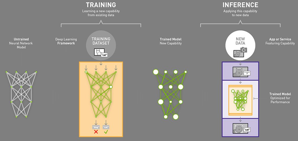
Graphic source: Nvidia Blog
This in turn has caused the industry to move towards inferencing on edge devices (consumer devices) because it’s a much more performant and power efficient. If you have your trained model on your device locally you can just use the processing power of the device to run the inference and avoid having to upload data to the cloud and have a server do it. This alleviates issues such as latency, bandwidth, and power consumption but also eliminates privacy concerns as the input data never leaves your device.
With the goal of running neural network inferencing locally on an edge device, we have the choice of running the implementation on various different processing blocks on devices such as a smartphone. CPU, GPU and even DSPs are all able to run inferencing tasks, however there are vast efficiency differences between them. General purpose CPUs are the least suited for the task as they are not designed with massive parallelised execution in mind. GPUs and DSPs are much better choices but even then there’s much room for improvement. It is here were we see a new class of processing accelerator like the NPU on the Kirin 970.
As these new IP blocks are still new the industry hasn’t had time to agree on a common nomenclature. HiSilicon/Huawei have coined the term NPU/neural processing unit while Apple publicly uses NE/neural engine. Other IP providers such as Cadence/Tensilica just outright call their implementation a neural network DSP (Vision C5), Imagination Technologies (Series 2NX) uses the term NNA/neural network accelerator and CEVA’s NeuPro settled on the marketing friendly “AI processor”. In the sense of simplicity I’ll just continue to refer to them as neural network IPs.
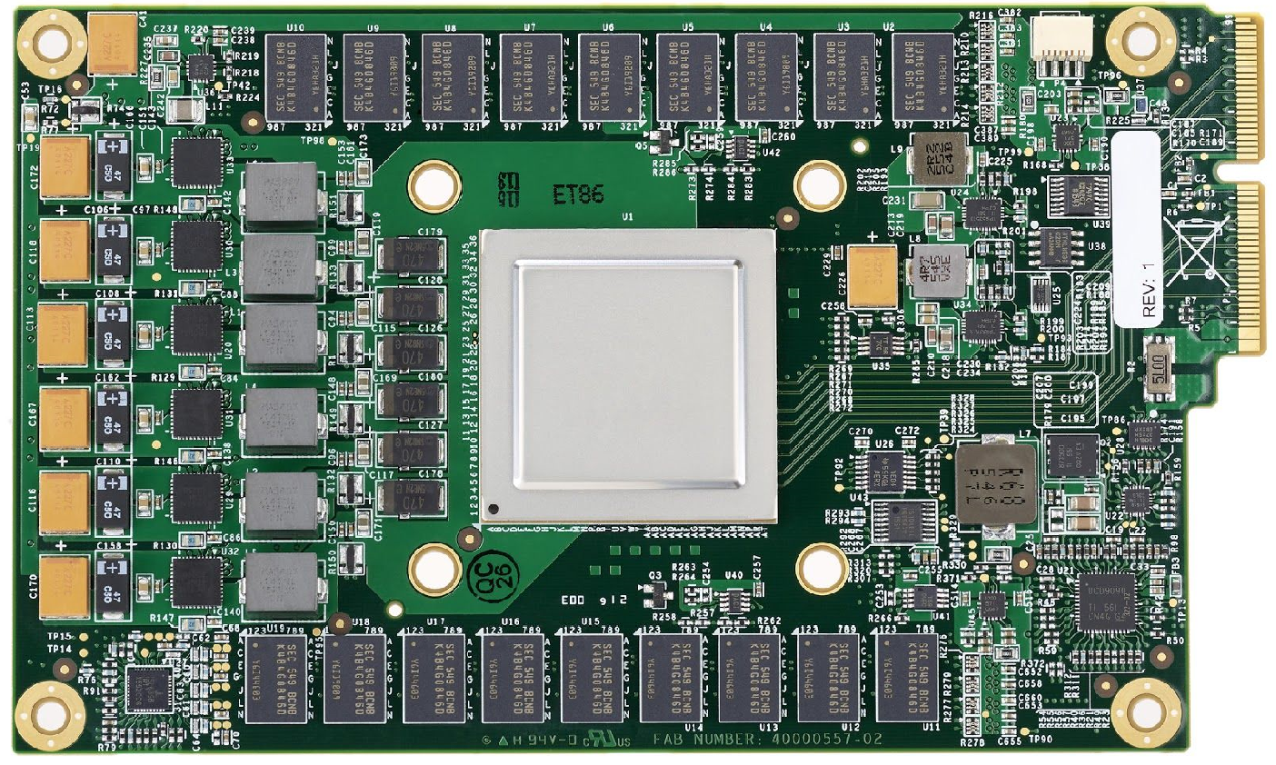
In the case of the Kirin 970 the NPU is provided by a new Chinese IP provider called Cambricon. The Kirin 970 NPU however isn’t a straight off-the-shelf offering but rather a co-development between Cambricon and HiSilicon optimized to HiSilicon’s requirements. Huawei quotes 2 TeraOPS FP16 performance on the IP, however this metric is misleading as the performance figure quotes sparse equivalent peak data, meaning the 8-bit quantized throughput. At this point in time we should largely shy away from theoretical performance figures of the neural network IPs as they don’t necessarily correlate to actual performance and there’s less understood architectural characteristics of the IPs that can play larger roles for the resulting end-performance.
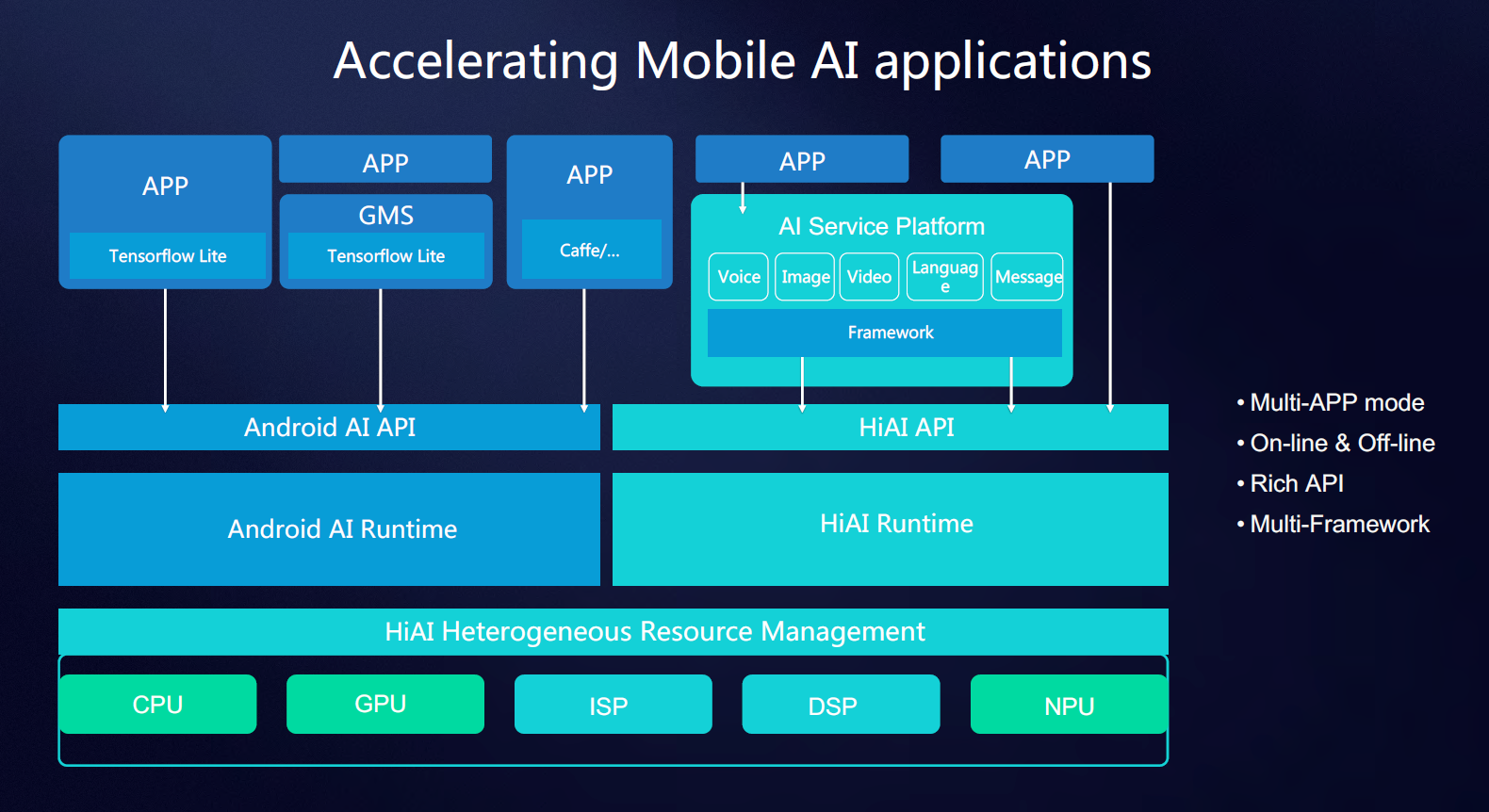
The first hurdle to using a neural network on a hardware block other than the CPU is to make use of the proper APIs to access that block. The SoC and IP vendors all currently ship proprietary APIs and SDKs to enable application development for using hardware acceleration for neural networks. In the case of HiSilicon they offer the HiAI API which can manage the workloads between CPU, GPU and NPU. The API is currently not publicly available as it’s still under development, but developers which reach out to HiSilicon can get early access before the public release later in the year. Vendors such as Qualcomm make available the SNPE (Snapdragon Neural Processing Engine) SDK which does the equivalent task of enabling app developers to tap into resources of the GPU and DSP for neural network processing workloads. Other IP vendors of course have their own SDKs for their respective IPs.
However vendor-specific APIs may end up being a temporary quirk of the present time; the goal in the future is to have a common universal API alongside the respective vendor’s IPs. Google has already been working on this and the NN API introduced in Android 8.1 is already actively shipping on Pixel 2 devices. One note that I’ve been made aware of is that currently the NN API only supports a subset of features that is available to IP like the NPU, so for developers to take full advantage of the hardware and extract maximum performance Huawei still sees application developers targeting the various proprietary APIs while using the NN API as a fall-back method.


116 Comments
View All Comments
StormyParis - Monday, January 22, 2018 - link
If the Modem IP is Huawei's one true in-house part, why didn't you at least test it alongside the CPU and GPU ? I'd assume in the real world, ti too has a large impact on batteyr and performance ?Ian Cutress - Monday, January 22, 2018 - link
The kit to properly test a modem power/attenuation to battery is around $50-100k. We did borrow one once, a few years ago, but it was only short-term loan. Not sure if/when we'll be able to do that testing again.juicytuna - Monday, January 22, 2018 - link
How does Mali have so many design wins? Why did Samsung switch from PowerVR to Mali? Cost savings? Politics? Because it clearly wasn't a descistion made on technical merit.lilmoe - Tuesday, January 23, 2018 - link
Because OEMs like Samsung are not stupid? And Mali is actually very power efficient and competitive?What are you basing your GPU decision on? Nothing in the articles provides evidence that Mali is less efficient than Adreno in UI acceleration or 60fps capped popular games (or even 60fps 1080p normalized T-Rex benchmark)...
Measuring the constant power draw of the GPU, which is supposed to be reached in vert short bursts, is absolutely meaningless.
lilmoe - Tuesday, January 23, 2018 - link
***Measuring the max (constant) power draw of the GPU, which is supposed to be reached in very short bursts during a workload, is absolutely meaningless.jospoortvliet - Saturday, January 27, 2018 - link
Your argument is half-way sensible for a CPU but not for a GPU.A GPU should not even HAVE a boost clock - there is no point in that for typical GPU workloads. Where a CPU is often active in bursts, a GPU has to sustain performance in games - normal UI work barely taxes it anyway.
So yes the max sustained performance and associated efficiency is ALL that matters. And MALI, at least in the implementations we have seen, is behind.
lilmoe - Sunday, January 28, 2018 - link
I think you're confusing fixed function processing with general purpose GPUs. Modern GPU clocks behave just like CPU cores, and yes, with bursts, just like NVidia's and AMD's. Not all scenes rendered in a game, for example, need the same GPU power, and not all games have the same GPU power needs.Yes, there is a certain performance envelope that most popular games target. That performance envelope/ target is definitely not SlingShot nor T-rex.
This is where Andrei's and your argument crumbles. You need to figure out that performance target and measure efficiency and power draw at that target. That's relatively easy to do; open up candy crush and asphalt 8 and measure in screen fps and power draw. That's how you measure efficiency on A SMARTPHONE SoC. Your problem is that you think people are using these SoCs like they would on a workstation. They don't. No one is going to render a 3dmax project on these phones, and there are no games that even saturate last year's flagship mobile gpu.
Not sure if you're not getting my simple and sensible point, or you're just being stubborn about it. Mobile SoC designed have argued for bursty gpu behavior for years. You guys need to get off your damn high horse and stop deluding yourself into thinking that you know better. What Apple or Qualcomm do isn't necessarily best, but it might be best for the gpu architecture THEY'RE using.
As for the CPU, you agree but Andrei insists on making the same mistake. You DON'T measure efficiency at max clocks. Again, max clocks are used in bursts and only for VERY short periods of time. You measure efficient by measuring the time it takes to complete a COMMON workload and the total power it consumes at that. Another hint, that common workload is NOT geekbench, and it sure as hell isn't SPEC.
lilmoe - Sunday, January 28, 2018 - link
The A75 is achieving higher performance mostly with higher clocks. The Exynos M3 is a wide core WITH higher clocks. Do you really believe these guys are idiots? You really think that's going to affect efficiency negatively? You think Android OEMs will make the same "mistake" Apple did and not provide adequate and sustainable power delivery?Laughable.
futrtrubl - Monday, January 22, 2018 - link
"The Kirin 970 in particular closes in on the efficiency of the Snapdragon 835, leapfrogging the Kirin 960 and Exynos SoCs."Except according to the chart right above it the 960 is still more efficient.
Andrei Frumusanu - Monday, January 22, 2018 - link
The efficiency axis is portrayed as energy (joules) per performance (test score). In this case the less energy used, the more efficient, meaning the shorter the bars, the better.