HiSilicon Kirin 970 - Android SoC Power & Performance Overview
by Andrei Frumusanu on January 22, 2018 9:15 AM ESTSPEC2006 - Full Results
The below chart might be a bit crowded but it it’s the only correct way to have a complete overview of the performance-power-efficiency triad of measurement metrics. The left axis dataset scales based on efficiency (Subtest total energy in joules / subtest SPECspeed score) and also includes the average active power usage (Watts) over the duration of the test. Here the shorter the bars the better the efficiency, while average power being a secondary metric but still should be below a certain value and well within the thermal envelope of a device. The right axis scales simply with the estimated SPECspeed score of the given test, the longer the bar the better the performance.
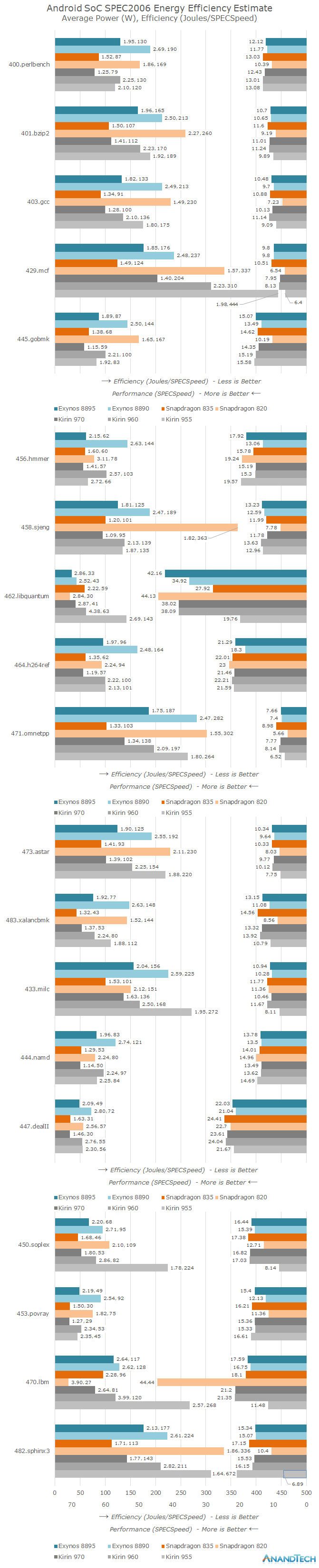
While the article is focused around the Kirin 970 improvements this is an invaluable opportunity to look back and the two last generations of devices from Qualcomm and Samsung. There is an immediate striking difference in the efficiency of the Snapdragon 820 and Snapdragon 835 across almost all subtests. The comparison between the Exynos 8890 and Snapdragon 820 variants of the S7 was an interesting debate at the time and we came to the conclusion the Exynos 8890 variant was the better unit as it offered longer battery life at higher performance. We see this represented in this dataset as well as the Exynos 8890 manages to have a measurable performance lead in a variety of tests while having higher energy efficiency, albeit a higher power envelope.
2017’s Galaxy S8 reversed this position as the Snapdragon 835 was clearly the better performing unit while having a slight battery life advantage. This efficiency delta can again be seen here as well as the Exynos 8895 isn’t able to compete with the lower power consumption of the Snapdragon 835, even though the performance differences between the Exynos M2 and Cortex A73 are a lot more of a wash than the previous generation’s battle between Exynos M1 and Kryo CPUs.
Switching over to the Kirin SoCs I included as far back as the Kirin 955 with the Cortex A72 as it was a very successful piece of silicon that definitely helped Huawei’s device portfolio for 2016. Remembering our coverage of the Cortex A73 microarchitecture we saw a lot of emphasis from ARM on the core’s floating point and memory subsystem performance. These claims can be easily confirmed when looking at the massive IPC gains in the memory access sensitive tests. When it comes to pure integer execution throughput the A72’s three-wide decoder as expected still managed to outpace the 2-wide unit on the A73 as seen in the 445.gobmk and 456.hmmer subtests.
The Kirin 960 was not able to always demonstrate ARM’s A73’s efficiency gains as again the more execution bound tests the Kirin 955 was equal or slightly more efficient. But again thanks to the new memory subsystem the A73 is able to well distance itself from the A72 with massive gains in 429.mcf, 433.milc, 450.soplex and 482.sphinx3. Again the power figures here are total platform active power so it’s also very possible that the Kirin 960’s memory controller could have a hefty part in the generational improvement.
The Kirin 970 doesn’t change the CPU IP, however we see the introduction of LPDDR4X on the memory controller side which will improve I/O power to the DRAM by lowering the voltage from 1.1V down to 0.6V. While performance should be the same power efficiency should thus be higher by the promised 20% that HiSilicon quotes from the switch to the TSMC 10nm process, plus some percentage due to LPDDR4X.
Performance indeed is within spitting distance of the Kirin 960, however it managed to be a few percentage points slower. On the power efficiency side we see large gains averaging up to 30% across the board. It looks that HiSilicon decided to invest all the process improvement into lowering overall power as the Kirin 970 manages to shave off a whole watt from the Kirin 960 both in integer and floating point benchmarks.
An interesting comparison here is the duel between the Snapdragon 835 and Kirin 970 – both A73 CPUs running at almost identical clocks, one manufactured on Samsung’s 10LPE process and the other on TSMC’s 10FF process. Again by making use of the various workload types we can extract information on the CPU and the memory sub-system. In 445.gobmk and 456.hmmer we see the Kirin have a very slight efficiency advantage at almost identical performance. This could be used as an indicator that TSMC’s process has a power advantage over Samsung’s process, something not too hard to imagine as the latter silicon was brought to market over half a year later.
When we however take a look at more memory bound tests we see the Snapdragon 835 overtake the Kirin 970 by ~20%. The biggest difference is in 429.mcf which is by far the most demanding memory test, and we see the Snapdragon 835 ahead by 32% in performance and a larger amount in efficiency. We can thus strongly assume that between the K970 and S835, Qualcomm has better and more efficient memory controller and subsystem implementation.
The memory subsystem generally seems to be the weak point of Samsung’s Exynos 8895. The M2 core remains competitive in execution bound tests however quickly falls behind in anything more memory demanding. The odd thing here is that I’m not sure if the reason here is memory controller inefficiency but rather something more related to the un-core of the M2 cluster. Firing up even integer power-viruses always have an enormous 1-core power overhead compared to the incremental power cost of additional threads on the remaining 3 cores. A hypothesis here is that given Samsung’s new Exynos 9810 makes use of a completely new cache hierarchy (all but confirmed a DynamiQ cluster) that the existing implementation in the M1 and M2 cores just didn’t see as much attention and design effort compared to the CPU core itself. Using a new efficient cluster design and continuing on improving the core might be how Samsung has managed to find a way (Gaining power and efficiency headroom) to double single-threaded performance in the Exynos 9810.
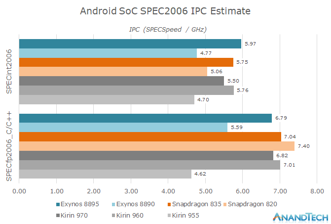
When overviewing IPC for SPEC2006, we see the Kirin 960 and Snapdragon 835 neck in neck, with the Kirin 970 being just slightly slower due to memory differences. The Exynos 8895 shows a 25% IPC uplift in CINT2006 and 21% uplift in CFP2006 whilst leading the A73 in overall IPC by a slight 3%.
The Snapdragon 820 still has good showing in terms of floating point performance thanks to Kryo’s four main “fat” execution pipelines can all handle integer as well as floating point operations. This theoretically should allow the core to have far more floating point execution power than ARM and Samsung’s cores, and is the explanation as to why 470.lbm sees such massive performance advantages on Kryo and brings up the overall IPC score.
The Final Overview
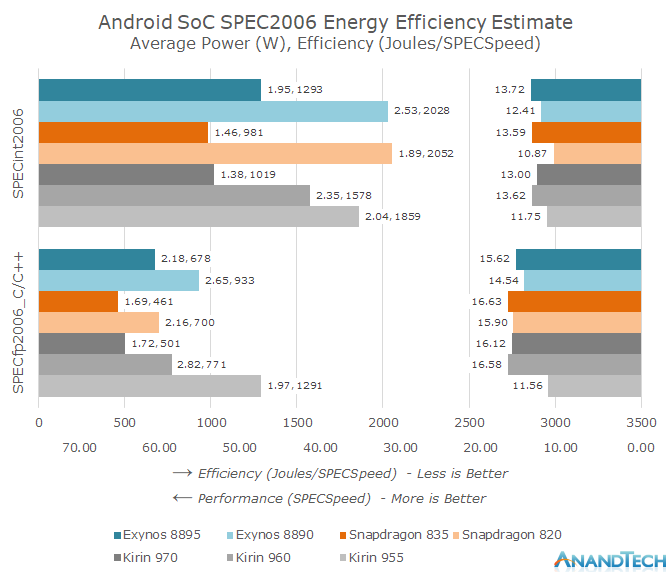
For a final overview of performance and efficiency we get to a mixed bag. If solely looking at the right axis with overall SPECspeed estimated results of CINT2006 and CFP2006, we see that performance hasn’t really moved much, if at all, over the last 2 generations. The Kirin 970 is a mere 10% faster than the Kirin 955 in CINT, over 2 years later. CFP sees larger gains over the A72 but again we come back to a small performance regression compared to the Kirin 960. If one would leave it at that then it’s understandable to raise the question as to what exactly is happening with Android SoC performance advancements.
For the most part, we’ve seen efficiency go up significantly in 2017. The Snapdragon 835 was a gigantic leap over the Snapdragon 820, doubling efficiency at a higher performance point in CINT and managing a 50% efficiency increase in CFP. The Exynos 8895 and Kirin 970 both managed to increase efficiency by 55% in CINT and the latter showed the same improvements in CFP.
This year’s SoCs have also seen a large decrease in average power usage. This bodes well for thermal throttling and flow low thermal envelope devices, as ARM had touted at the launch of the A73. The upcoming Snapdragon 845 and A75 cores promise no efficiency gains over the A73, so the improved performance comes with linear increase in power usage.
I’m also not too sure about Samsung’s Exynos 9810 claiming such large performance jumps and just hope that those peak 2.9GHz clocks don’t come with outrageous power figures just for the sake of benchmark battling with Apple. The Exynos’ 8890 2-core boost feature was in my opinion senseless as the performance benefit of the additional 300MHz was not worth the efficiency penalty (The above results were run at the full 2.6GHz, 2.3GHz is only 10% slower but 25% more efficient) and the whole thing probably had more to do with matching the Snapdragon 820’s scores in the flawed GeekBench 3.
I’m not too sure how to feel about that as I think the current TDPs of the Snapdragon 835 and Kirin 970 (in CPU workloads) are sweet spots that the industry should maintain as it just gives a better mobile experience to the average user, so I do really hope the Snapdragon 845 offers some tangible process improvements to counter-act the micro-architectural power increase as well as clock increases otherwise we’ll see power shooting up again above 2W.


116 Comments
View All Comments
StormyParis - Monday, January 22, 2018 - link
If the Modem IP is Huawei's one true in-house part, why didn't you at least test it alongside the CPU and GPU ? I'd assume in the real world, ti too has a large impact on batteyr and performance ?Ian Cutress - Monday, January 22, 2018 - link
The kit to properly test a modem power/attenuation to battery is around $50-100k. We did borrow one once, a few years ago, but it was only short-term loan. Not sure if/when we'll be able to do that testing again.juicytuna - Monday, January 22, 2018 - link
How does Mali have so many design wins? Why did Samsung switch from PowerVR to Mali? Cost savings? Politics? Because it clearly wasn't a descistion made on technical merit.lilmoe - Tuesday, January 23, 2018 - link
Because OEMs like Samsung are not stupid? And Mali is actually very power efficient and competitive?What are you basing your GPU decision on? Nothing in the articles provides evidence that Mali is less efficient than Adreno in UI acceleration or 60fps capped popular games (or even 60fps 1080p normalized T-Rex benchmark)...
Measuring the constant power draw of the GPU, which is supposed to be reached in vert short bursts, is absolutely meaningless.
lilmoe - Tuesday, January 23, 2018 - link
***Measuring the max (constant) power draw of the GPU, which is supposed to be reached in very short bursts during a workload, is absolutely meaningless.jospoortvliet - Saturday, January 27, 2018 - link
Your argument is half-way sensible for a CPU but not for a GPU.A GPU should not even HAVE a boost clock - there is no point in that for typical GPU workloads. Where a CPU is often active in bursts, a GPU has to sustain performance in games - normal UI work barely taxes it anyway.
So yes the max sustained performance and associated efficiency is ALL that matters. And MALI, at least in the implementations we have seen, is behind.
lilmoe - Sunday, January 28, 2018 - link
I think you're confusing fixed function processing with general purpose GPUs. Modern GPU clocks behave just like CPU cores, and yes, with bursts, just like NVidia's and AMD's. Not all scenes rendered in a game, for example, need the same GPU power, and not all games have the same GPU power needs.Yes, there is a certain performance envelope that most popular games target. That performance envelope/ target is definitely not SlingShot nor T-rex.
This is where Andrei's and your argument crumbles. You need to figure out that performance target and measure efficiency and power draw at that target. That's relatively easy to do; open up candy crush and asphalt 8 and measure in screen fps and power draw. That's how you measure efficiency on A SMARTPHONE SoC. Your problem is that you think people are using these SoCs like they would on a workstation. They don't. No one is going to render a 3dmax project on these phones, and there are no games that even saturate last year's flagship mobile gpu.
Not sure if you're not getting my simple and sensible point, or you're just being stubborn about it. Mobile SoC designed have argued for bursty gpu behavior for years. You guys need to get off your damn high horse and stop deluding yourself into thinking that you know better. What Apple or Qualcomm do isn't necessarily best, but it might be best for the gpu architecture THEY'RE using.
As for the CPU, you agree but Andrei insists on making the same mistake. You DON'T measure efficiency at max clocks. Again, max clocks are used in bursts and only for VERY short periods of time. You measure efficient by measuring the time it takes to complete a COMMON workload and the total power it consumes at that. Another hint, that common workload is NOT geekbench, and it sure as hell isn't SPEC.
lilmoe - Sunday, January 28, 2018 - link
The A75 is achieving higher performance mostly with higher clocks. The Exynos M3 is a wide core WITH higher clocks. Do you really believe these guys are idiots? You really think that's going to affect efficiency negatively? You think Android OEMs will make the same "mistake" Apple did and not provide adequate and sustainable power delivery?Laughable.
futrtrubl - Monday, January 22, 2018 - link
"The Kirin 970 in particular closes in on the efficiency of the Snapdragon 835, leapfrogging the Kirin 960 and Exynos SoCs."Except according to the chart right above it the 960 is still more efficient.
Andrei Frumusanu - Monday, January 22, 2018 - link
The efficiency axis is portrayed as energy (joules) per performance (test score). In this case the less energy used, the more efficient, meaning the shorter the bars, the better.