Ryzen Mobile is Launched: AMD APUs for Laptops, with Vega and Updated Zen
by Ian Cutress on October 26, 2017 9:00 AM ESTManaging Power
When designing a processor, power delivery is as important as the microarchitecture. There are many ways to provide power, with the options typically balancing design effort, die area, efficiency, and simplicity.
The best way to look at it is to consider a basic implementation. This might be to supply one power rail to all cores with one set voltage to all of them, and a separate power rail to the graphics, and a separate power rail to the memory controller. Let the motherboard manage the input voltages into the chip, and controlling each large segment is easy. Now how about separating up each of the cores into its own voltage island, and being able to control them all individually. This design is more complex, requires more control, but ultimately can be used to save a lot of power – there is no need to fire up all the cores to 4.0 GHz when only one is active. The downside of this implementation is if the design needs a separate power rail for each core coming into the processor. This makes the motherboard side of the power regulation very complex and expensive, and potentially inefficient.
The next step in the design would be to create a single voltage rail going into processor, and sorting out the voltages inside the processor with regulators. It sounds complex to do in silicon because it is, but offers the best payoffs. AMD has done that last one.
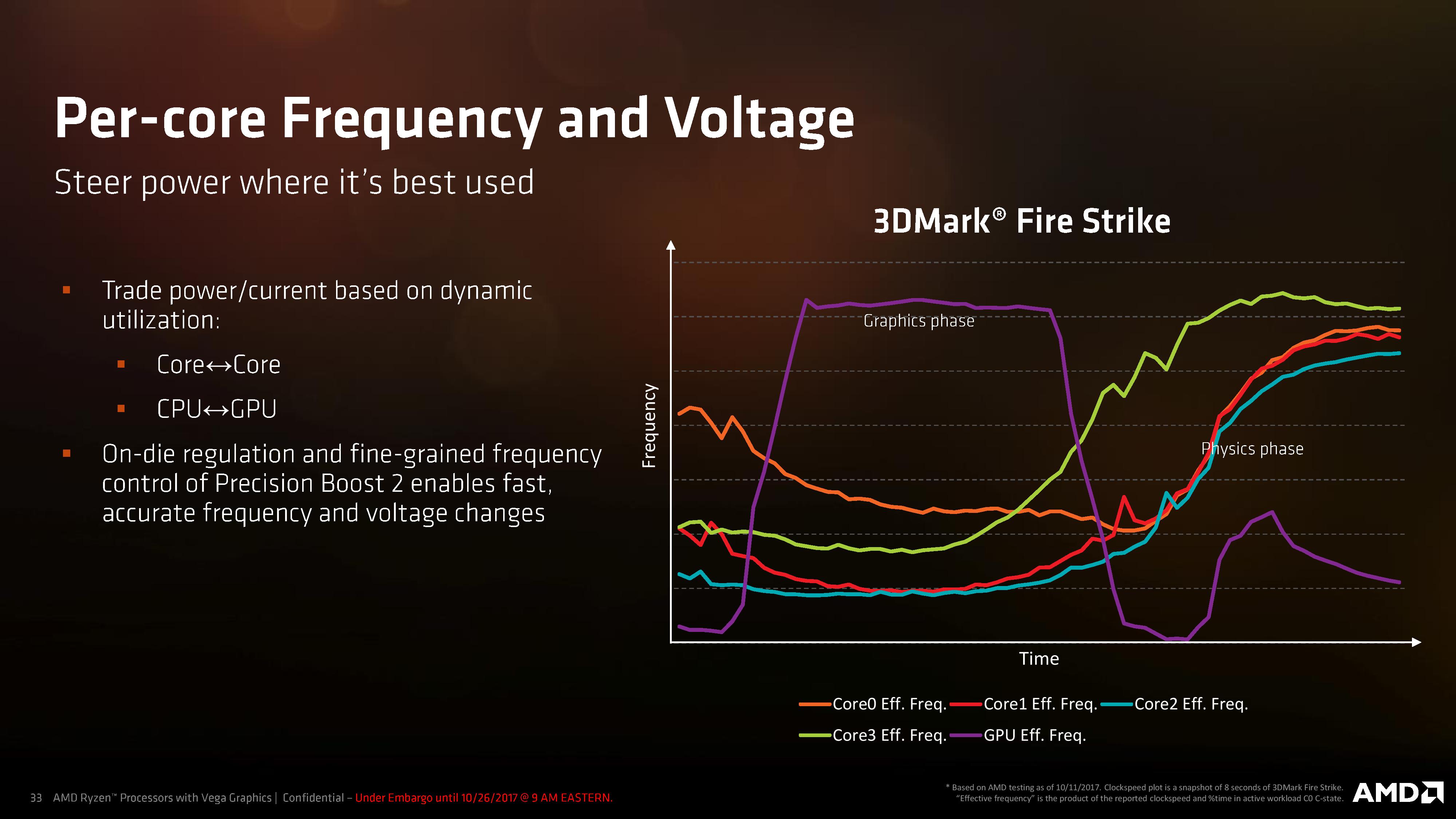
The biggest upside to such a design is sending power where it needs to go while also keeping costs down and efficiency high. With all the effort in the design phase, it becomes a better platform when put into the field. In this slide, AMD shows how the processor keeps one core half-fed and another core ticking over during the graphics phase of 3DMark, while they issue kernel commands and do some basic physics, but when the physics phase kicks in the cores can each turbo individually while the GPU comes back down. Add in some fine-grained control and as long as it reacts quick enough, it should offer a power-efficient implementation.
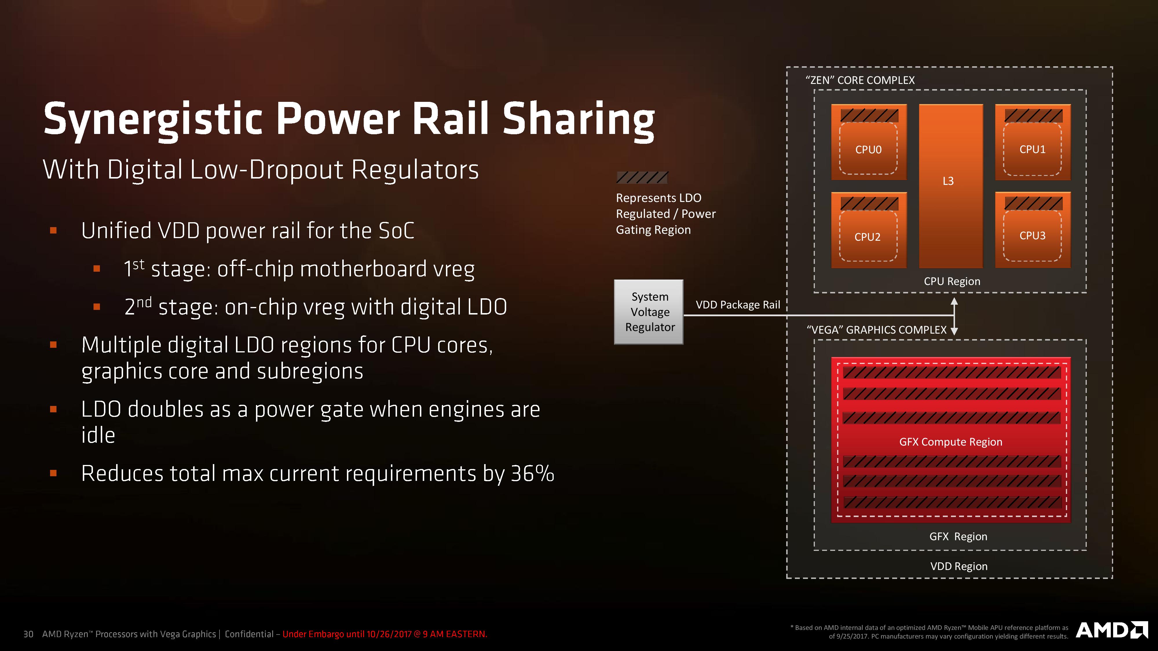
AMD calls the first part of what they have done as ‘Synergistic Power Rail Sharing’, which basically means one power rail going into the processor. If that sounds familiar, Intel did it with Broadwell and currently does it on their high-end processors. Where Intel used a FIVR, or fully integrated voltage regulator with massive inductors (remember the cut out required on Broadwell motherboards for those inductors?), AMD is using a split VDD package rail and per-island linear low-dropout regulators (LDO) for each of the cores and each of the compute units. Every voltage island required gets an optimized LDO for its purpose, which doubles as a power gate when that portion of the processor can be turned off. This implementation allows for the motherboard to be simplified (lower cost), and the processor to have better control, at the expense of extra control circuitry.
When Intel introduced their FIVR implementation, they said that they found better efficiency using their big inductors and decided against the linear LDO regulators because they were inefficient at low power. We put that to Sam Naffziger, AMD’s top guy on power, and he responded that yes, as a percentage, the power efficiency at idle might be lower than expected – but the power consumption of an idle core while another is loaded is still a very tiny proportion. Sam stated that when the LDO is in complete power gate mode, it can be considered off and any residual power consumption is minimal, regardless of its actual efficiency. He said that they still worked hard on the LDO implementation for power efficiency anyway, to make sure everything still worked. Overall, total current requirements were down 36%, which reduces the motherboard-side power regulation, leading to smaller, lighter, and potentially cooler designs.
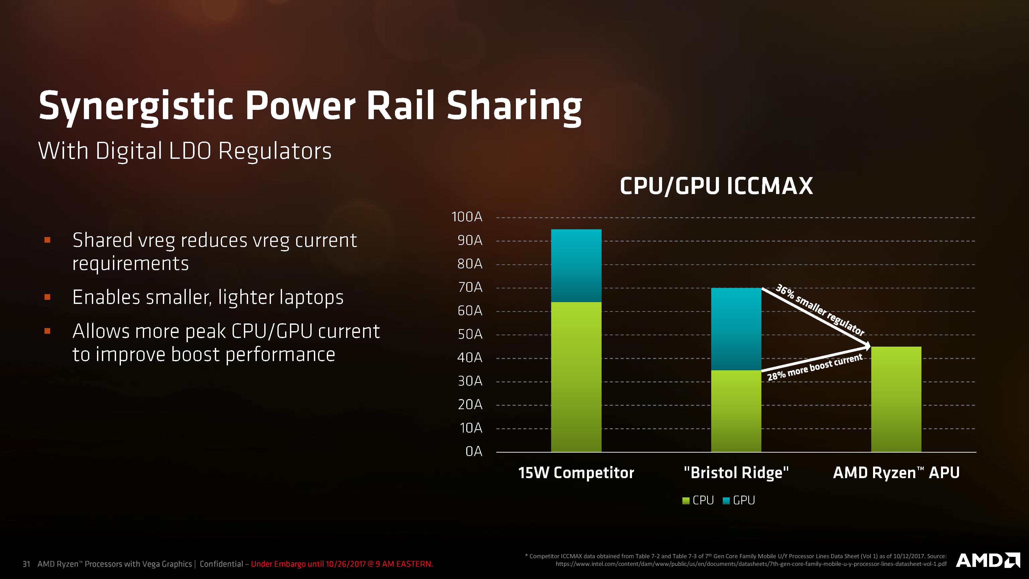
AMD stated that with Intel’s new 8th Generation Kaby Lake-R mobile processors, with the increase in core count but the same TDP, it meant that the system had to drive more current, especially to hit the higher PL2 power state which had more than doubled over the 7th generation parts. The downside to having a single rail implementation, at least from a reviewer’s perspective, is that it now becomes harder to separate the CPU and the GPU for power monitoring.

With per-core voltage access, AMD is able to fine-tune the dynamic voltage/frequency scaling algorithms for each core as well as the GPU based on the external sensors, current loading, and available power. As long as threads are not jumping from core to core, AMD is able to identify the cores that are churning through the most work (e.g. during a game) and direct power to those cores using frequency arbiters for each core.
Race to Sleep
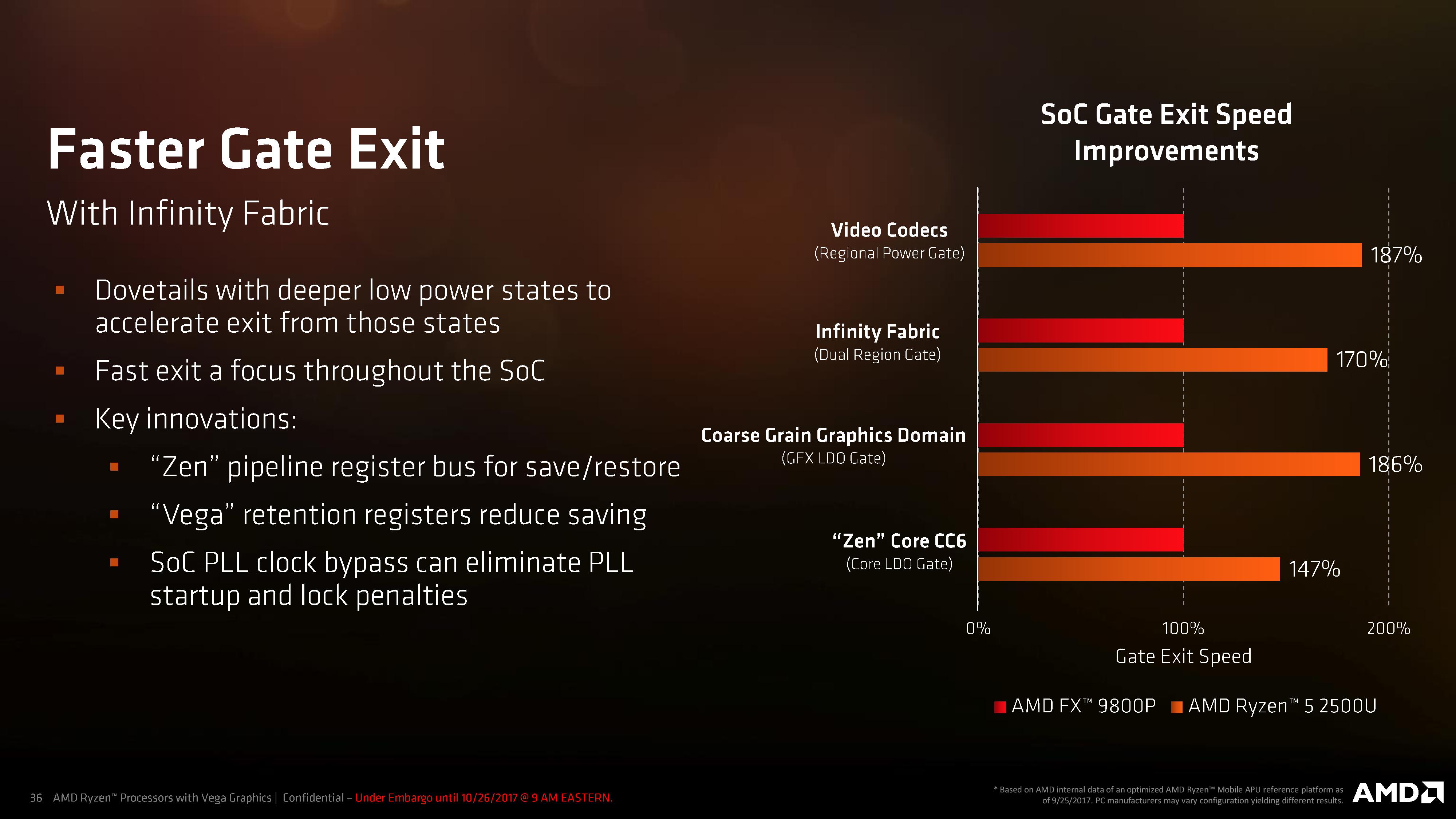
In the past we had the race to idle – the notion that if you applied extra power to finish a workload quicker, overall less energy was used when you compared the static (always there) and dynamic (on demand) energy of the system. Now we have a race-to-sleep: how quickly can the parts of the chip come in and out of sleep states in order to save power. If one element of the silicon gets a request every 50ms that takes 25ms to process, it has a 25ms window to potentially sleep – if it can’t get in and out of sleep in under 10ms, then there is no point turning it off.
The race to sleep is usually countered by offering a series of sleep states, with the nearest sleep states being quicker to enter/exit but offering less of a power reduction. With Ryzen Mobile, AMD is adding extra sleep states due to the use of the linear LDO regulators we discussed in the previous section.
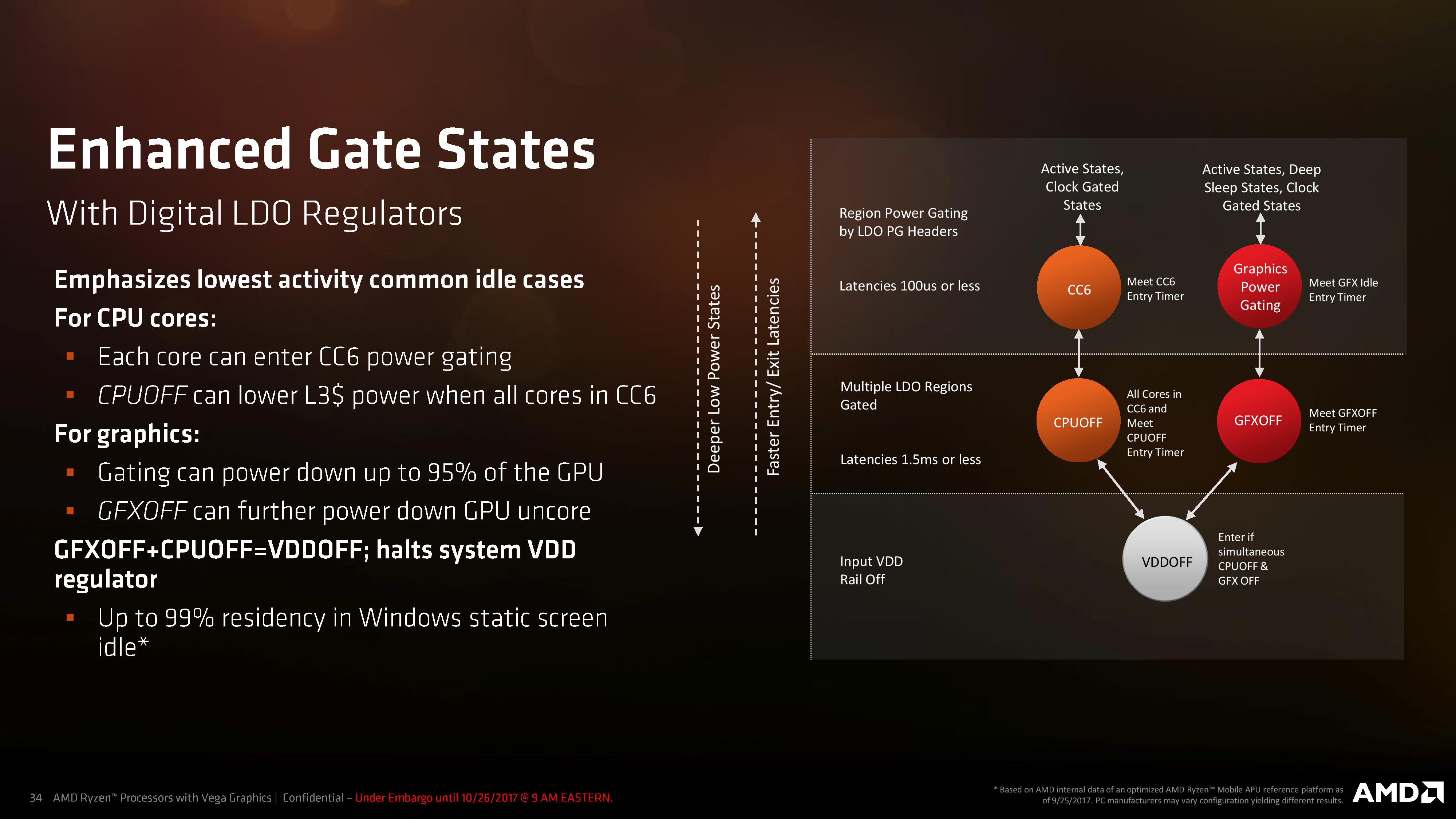
With each core now in its own power island with its own LDO, each core can enter sleep states independently. In this case, AMD’s CC6 state powers off most of the core but keeps the L3 cache active in case another CPU uses it – it only takes 100 microseconds to enter/exit this CC6 state. When all the cores are in CC6, the regulators can also disable the L3 cache altogether for a CPUOFF state, giving better power reductions but now the entry/exist latency is around 1.5ms.
The same goes for the graphics: the LDO regulators can effectively power gate 95% of the GPU, including the compute units, the fixed function encoders/decoders, and potentially parts of the display pipeline. The uncore is still active however, in case other parts of the GPU need to use it. When certain criteria are met, the graphics can enter a GFXOFF state, saving most of the power.
When CPUOFF and GFXOFF are both enabled, the system can fully implement VDDOFF, which disables most of the processor entirely. This sounds like a complete system shutdown, but enough of the display pipeline is active to still have a powered on state. AMD is quoting that when a system has a static Windows screen with nothing firing up the cores, the chip could be in this VDDOFF state up to 99% of the time.
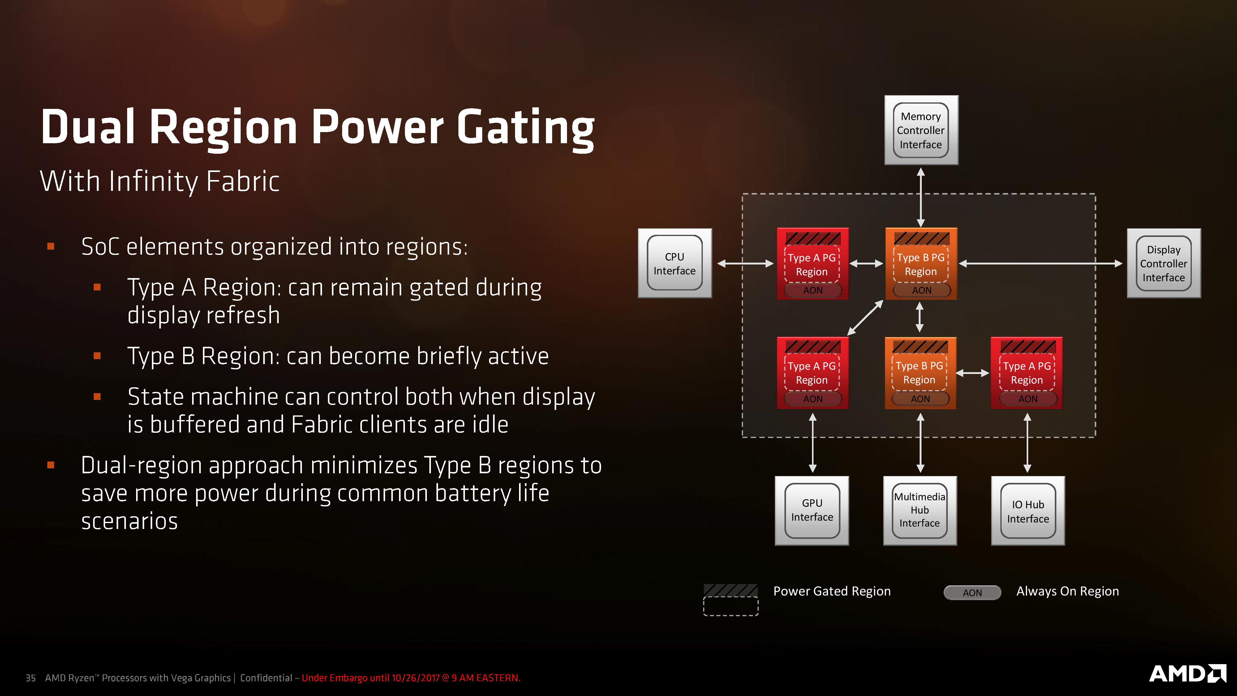
Some of this power gating control comes through the Infinity Fabric, which consists of both data control and system control elements. As some of the regions of the processor still need to remain on to keep the system alive, even in VDDOFF mode, AMD has used the Infinity Fabric to separate the core into two different sorts of regions:
Type A: Can remain off during display refresh
Type B: Can become briefly active for display refresh
Because a 60 Hz panel will refresh every 16.6ms, certain parts of the SoC still need to ensure the frame buffer has data and keep it active. Obviously, if the data buffer needs updating then a lot more of the processor needs to fire up to do so, but this case is taking care more about static images on the display, and overall is an intersting approach that is something we more typically see in smartphone/tablet-focused processors.
With the two region types, the fewer Type B regions there are means the more power you can save by keeping the Type A regions turned off during display refreshes. In this case AMD uses a state machine to control the display buffer and keep control of the different regions, but here it shows that only the memory controller, display controller, and multimedia hub are in that Type-B for display refreshes, and the rest of the processor can remain in the lower power states.
This ultimately saves more power for laptops when it comes to battery life: how much of the time does a user spend on a laptop just looking/reading at a static screen? It is a very common use case.
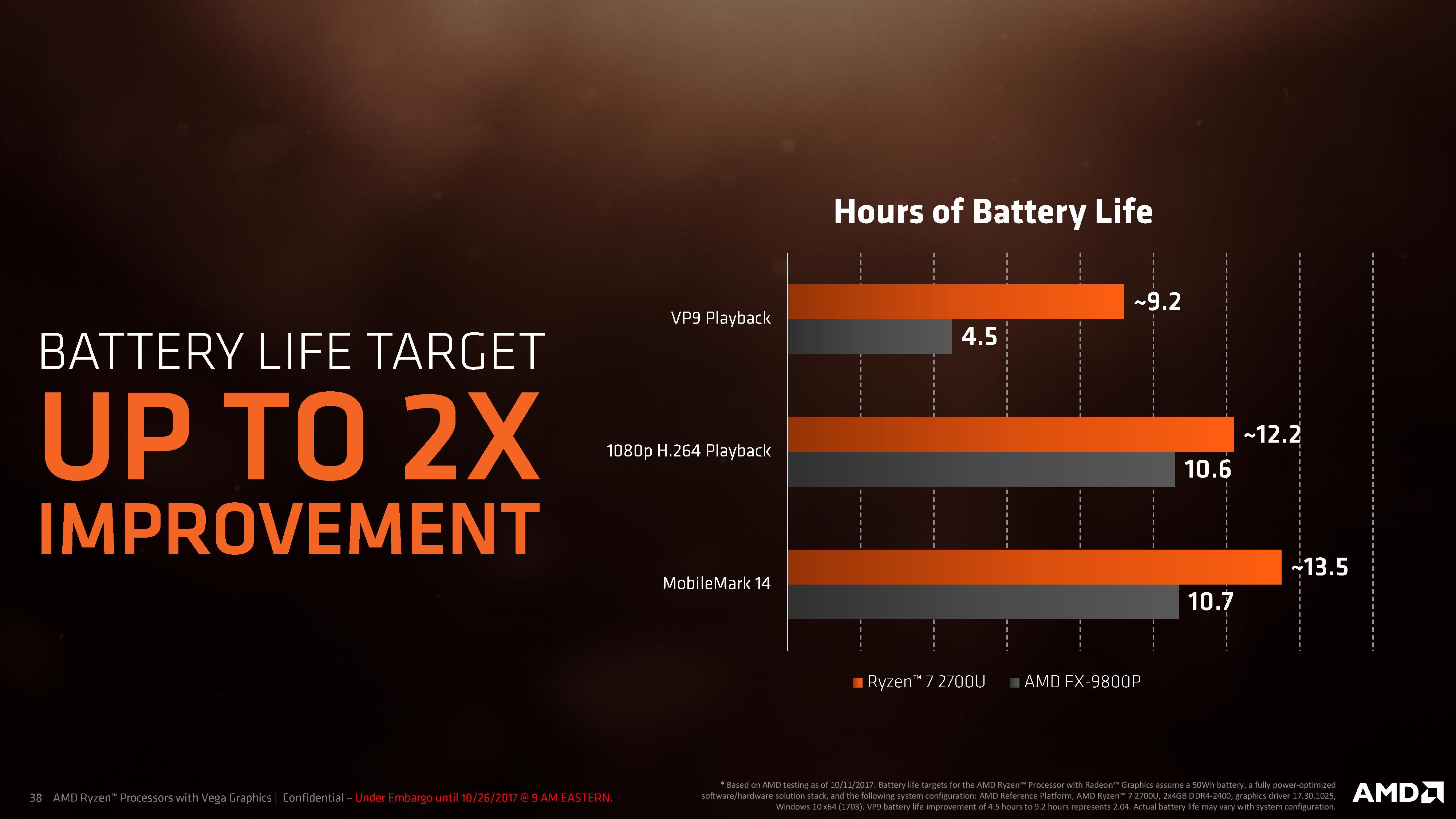
Ultimately AMD is saying that with all the new power enhancements, they are expecting good improvements in battery life. With this slide, VP9 playback time is doubled (because now the GPU has a VP9 decoder); while something more comparable like 1080p H264 playback is boosted by 15%. That doesn’t sound like much, but it can mean an extra few minutes when you are running low trying to get something done in a high-pressure situation.


140 Comments
View All Comments
jjj - Thursday, October 26, 2017 - link
It's on 14nm,the actual silicon is maybe 15$ and then there is test and packaging.The cost of the die is not much of an issue.They can easily price the average SKU between 80-100$ with the fastest SKUs a bit above and the lesser SKUs bellow. Not that Intel has much different pricing, the prices they list have nothing to do with reality,.wumpus - Thursday, October 26, 2017 - link
While it likely costs the same to make as a R3 Ryzen (closer to an R7, because all CPU cores have to work), it will take a long time to dig themselves out of their hole by pricing it at $80-100.Don't forget they have to pay for the mask with "ryzen mobile" sales, while ryzen and epyc paid for Zepplin die tooling. I don't expect it to be a cheap chip unless AMD is absolutely forced to (like they have been forced to for years and are hungry for Intel level margins).
velanapontinha - Thursday, October 26, 2017 - link
A very small difference between both processors, yet one is Ryzen 5 and the other is Ryzen 7. I really hope these are the lowest R7 and the highest R5.zodiacfml - Friday, October 27, 2017 - link
Appears to me that these are the best parts already. I can get by with a mobile R3 without hyperthreading.stanleyipkiss - Thursday, October 26, 2017 - link
A 14" Acer Swift 3 with the Kaby Lake-R (4 core/8 thread) 8 GB RAM and a MX150 from nVidia gets better FPS in every game outlined by AMD here. Why go for this? It's not lighter, it's not more efficient, it's not faster.In the real world, GPU performance is sub-par a 1030 (MX150). The only upside is the fact that you don't have to deal with Intel's iGPU and nVidia's discrete GPU in the same package. Other than that... not worth the hassle.
BrokenCrayons - Thursday, October 26, 2017 - link
There appears to be a power advantage over a KB + MX150 since the combined consumption of the CPU and dGPU are higher than mobile Ryzen alone. All things equal, you're going to give up some GPU performance in exchange for more battery life. It's a trade-off some people will be willing to make and others will reject. Cool either way, just buy what works best for you and don't worry about it.With that said, I think Vega would do better with dedicated video memory of some sort which is why I would have liked to see these chips released with a small HBM cache that can be used to supplement the system's DDR4, but that's probably an unrealistic pipe dream for the time being. The added costs of associated would make mobile Ryzen more expensive...maybe more than a CPU + dGPU combination capable of the same performance.
Jon Tseng - Thursday, October 26, 2017 - link
Anyone got any hard numbs on how this compares to KBL + MX150? I saw some commentary that Ryzen Mobile was comparable to the 950M... IIRC MX150 was a perf bump on the old 940MX. So are they on a similar level or does MX150 have a material advantage?Was thinking that if they are in the same zip code perf wise then Ryzen is a no brainer given power draw..
stanleyipkiss - Thursday, October 26, 2017 - link
The MX150 is on par if not better than the old 960M. It's a huge step up from all iGPUs.BrokenCrayons - Thursday, October 26, 2017 - link
The 960M is consistently faster in synthetics (by a small margin) and in gaming benchmarks (by a much larger margin) than the MX150. Here's a couple of notebookcheck links to compare:https://www.notebookcheck.net/NVIDIA-GeForce-GTX-9...
https://www.notebookcheck.net/NVIDIA-GeForce-MX150...
vladx - Thursday, October 26, 2017 - link
Indeed GPU performance is vey dissapointing, but par for the course for Vega.