The AnandTech Coffee Lake Review: Initial Numbers on the Core i7-8700K and Core i5-8400
by Ian Cutress on October 5, 2017 9:00 AM EST- Posted in
- CPUs
- Intel
- Core i5
- Core i7
- Core i3
- 14nm
- Coffee Lake
- 14++
- Hex-Core
- Hyperthreading
Silicon and Process Nodes: 14++
Despite being somewhat reserved in our pre-briefing, and initially blanket labeling the process node for these chips as ‘14nm’, we can confirm that Intel’s newest ‘14++’ manufacturing process is being used for these 8th Generation processors. This becomes Intel’s third crack at a 14nm process, following on from Broadwell though Skylake (14), Kaby Lake (14+), and now Coffee Lake (14++).
With the 8th Generation of processors, Intel is moving away from having the generation correlate to both the process node and microarchitecture. As Intel’s plans to shrink its process nodes have become elongated, Intel has decided that it will use multiple process nodes and microarchitectures across a single generation of products to ensure that every update cycle has a process node and microarchitecture that Intel feels best suits that market. A lot of this is down to product maturity, yields, and progress on the manufacturing side.
| Intel's Core Architecture Cadence (8/20) | |||||
| Core Generation | Microarchitecture | Process Node | Release Year | ||
| 2nd | Sandy Bridge | 32nm | 2011 | ||
| 3rd | Ivy Bridge | 22nm | 2012 | ||
| 4th | Haswell | 22nm | 2013 | ||
| 5th | Broadwell | 14nm | 2014 | ||
| 6th | Skylake | 14nm | 2015 | ||
| 7th | Kaby Lake | 14nm+ | 2016 | ||
| 8th | Kaby Lake Refresh Coffee Lake Cannon Lake |
14nm+ 14nm++ 10nm |
2017 2017 2018? |
||
| 9th | Ice Lake? ... |
10nm+ | 2018? | ||
| Unknown | Cascade Lake (Server) | ? | ? | ||
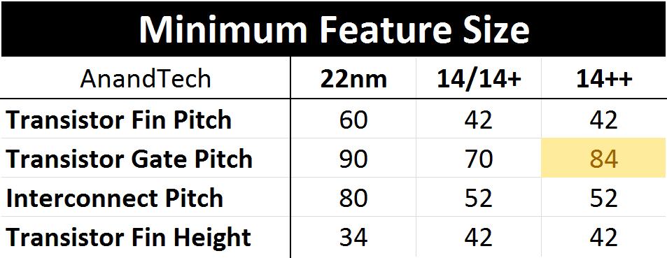
Kaby Lake was advertised as using a 14+ node with slightly relaxed manufacturing parameters and a new FinFET profile. This was to allow for higher frequencies and better overclocking, although nothing was fundamentally changed in the core manufacturing parameters. With Coffee Lake at least, the minimum gate pitch has increased from 70nm for 84nm, with all other features being equal.
Increased gate pitch moves transistors further apart, forcing a lower current density. This allows for higher leakage transistors, meaning higher peak power and higher frequency at the expense of die area and idle power.
Normally Intel aims to improve their process every generation, however this seems like a step ‘back’ in some of the metrics in order to gain performance. The truth of the matter is that back in 2015, we were expecting Intel to be selling 10nm processors en-masse by now. As delays have crept into that timeline, the 14++ note is holding over until 10nm is on track. Intel has already stated that 10+ is likely to be the first node on the desktop, which given the track record on 14+ and 14++ might be a relaxed version of 10 in order to hit performance/power/yield targets, with some minor updates. Conceptually, Intel seems to be drifting towards seperate low-power and high-performance process nodes, with the former coming first.
Of course, changing the fin pitch is expected to increase the die area. With thanks to HEKPC (via Videocardz), we can already see a six-core i7-8700K silicon die compared to a quad-core i7-7700K.
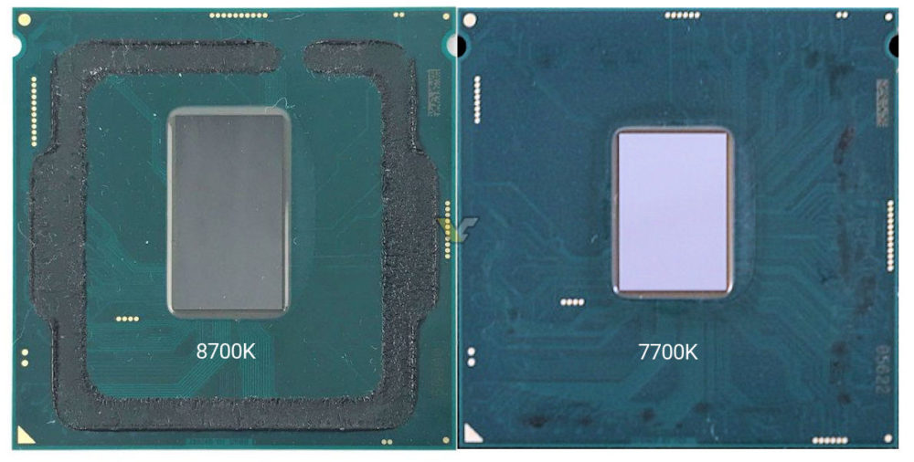
The die area of the Coffee Lake 6+2 design (six cores and GT2 graphics) sits at ~151 mm2, compared to the ~125 mm2 for Kaby Lake 4+2 processor: a 26mm2 increase. This increase is mainly due to the two cores, however there is a minor adjustment in the integrated grpahics as well to support HDCP 2.2, not to mention any unpublished changes Intel has made to their designs between Kaby Lake and Coffee Lake.
The following calculations are built on assumptions and contain a margin of error
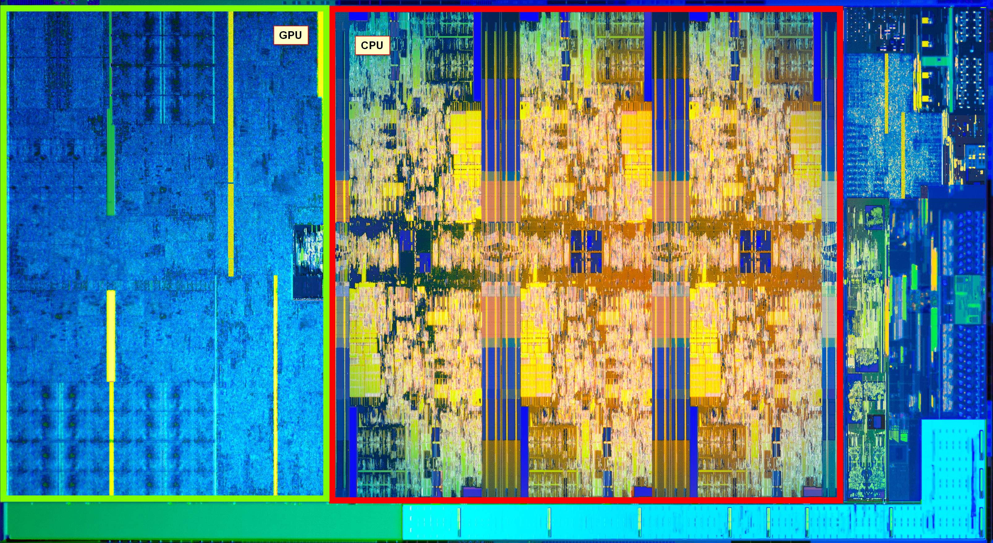
With the silicon floor plan, we can calculate that the CPU cores (plus cache) account for 47.3% of the die, or 71.35 mm2. Divided by six gives a value of 11.9 mm2 per core, which means that it takes 23.8 mm2 of die area for two cores. Out of the 26mm2 increase then, 91.5% of it is for the CPU area, and the rest is likely accounting for the change in the gate pitch across the whole processor.
The Coffee Lake 4+2 die would then be expected to be around ~127 mm2, making a 2mm2 increase over the equivalent Kaby Lake 4+2, although this is well within the margin of error for measuring these processors. We are expecting to see some overclockers delid the quad-core processors soon after launch.
In previous Intel silicon designs, when Intel was ramping up its integrated graphics, we were surpassing 50% of the die area being dedicated to graphics. In this 6+2 design, the GPU area accounts for only 30.2% of the floor plan as provided, which is 45.6 mm2 of the full die.
Memory Support on Coffee Lake
With a new processor generation comes an update to memory support. There is always a small amount of confusion here about what Intel calls ‘official memory support’ and what the processors can actually run. Intel’s official memory support is typically a guarantee, saying that in all circumstances, with all processors, this memory speed should work. However motherboard manufacturers might offer speeds over 50% higher in their specification sheets, which Intel technically counts as an overclock.
This is usually seen as Intel processors having a lot of headroom to be conservative, avoid RMAs, and maintain stability. In most cases this is usually a good thing: there are only a few niche scenarios where super high-speed memory can equate to tangible performance gains* but they do exist.
*Based on previous experience, but pending a memory scaling review
For our testing at least, our philosophy is that we test at the CPU manufacturers’ recommended setting. If there is a performance gain to be had from slightly faster memory, then it pays dividends to set that as the limit for official memory support. This way, there is no argument on what the rated performance of the processor is.
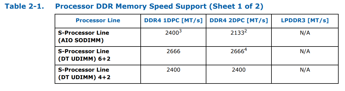
For the new generation, Intel is supporting DDR4-2666 for the six-core parts and DDR4-2400 for the quad-core parts, in both 1DPC (one DIMM per channel) and 2DPC modes. This should make it relatively simple, compared to AMD’s memory support differing on DPC and type of memory.
It gets simple until we talk about AIO designs using the processors, which typically require SODIMM memory. For these parts, for both quad-core and hex-core, Intel is supporting DDR4-2400 at 1DPC and DDR4-2133 at 2DPC. LPDDR3 support is dropped entirely. The reason for supporting a reduced memory frequency in an AIO environment with SODIMMs is because these motherboards typically run their traces as chained between the memory slots, rather than a T-Topology which helps with timing synchronization. Intel has made the T-Topology part of the specification for desktop motherboards, but not for AIO or integrated ones, which explains the difference in DRAM speed support.
These supported frequencies follow JEDEC official sub-timings. Familiar system builders will be used to DDR4-2133 at a CAS Latency of 15, but as we increase the speed of the modules, the latency increases to compensate:
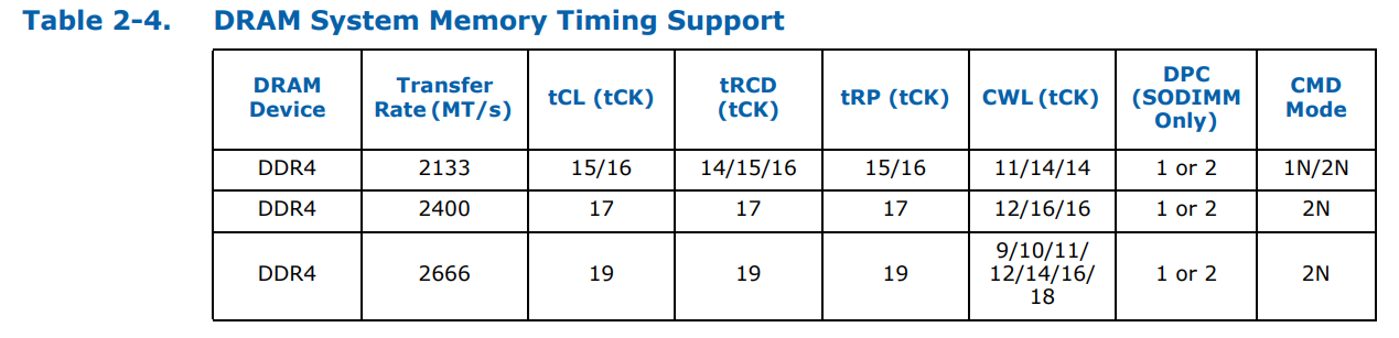
Intel’s official sub-timing support at DDR4-2666 is 19-19-19. Outside of enterprise modules, that memory does not really exist, because memory manufacturers can seem to mint DDR4-2666 16-17-17 modules fairly easily, and these processors are typically fine with those sub-timings. CPU manufacturers typically only state ‘supported frequency at JEDEC sub-timings’ and do not go into sub-timing discussions, because most users care more about the memory frequency. If time permits, it would be interesting to see just how much of a performance deficit the official JEDEC sub-timings provide compared to what memory is actually on sale.


222 Comments
View All Comments
boeush - Friday, October 6, 2017 - link
To expand on this a bit more, with the "core wars" now in effect, I wonder if hyperthreading might be an unnecessary holdover feature that could be actually reducing performance of many(8+)-core chips in all but the most extremely threaded scenarios. Might it not be better to have many simple/efficient cores, rather than perhaps fewer cores loaded with the hyperthreading overhead both in terms of die area and energy density, as well as cache thrashing?Zingam - Saturday, October 7, 2017 - link
Hyperthreading was invented to optimize the use of CPU logic that would otherwise remain unutilized during high loads.There is no way of reducing performance with current architectures. There are "hyperthreading-less" CPUs and you compare them to hyperthreded CPUs.boeush - Monday, October 9, 2017 - link
Hyperthreading was particularly useful in the context of not having a lot of cores to work with - allowing to squeeze extra multi-threaded performance from your dual- or quad-core CPU. It comes at the cost of extra silicon and complexity in the CPU pipeline, but allows better utilization of CPU resources as you mention. At runtime, it has the dual detrimental effects on single-thread performance, of (1) splitting/sharing the on-CPU cache among more threads, thereby raising the frequency of cache misses for any given thread due to the threads trampling over each other's cached data, and (2) indeed maximizing CPU resource utilization, thereby maximizing dissipated energy per unit area - and thereby driving the CPU into a performance-throttling regime.With more cores starting to become available per CPU in this age of "core wars", it's no longer as important to squeeze every last ounce of resource utilization from each core. Most workloads/applications are not very parallelizable in practice, so you end up hitting the limits of Amdahl's law - at which point single-thread performance becomes the main bottleneck. And to maximize single-thread performance on any given core, you need two things: (a) maximum attainable clock frequency (resource utilization be damned), and (b) as much uncontested, dedicated on-CPU cache as you can get. Hyperthreading is an impediment to both of those goals.
So, it seems to me that if we're going toward the future where we routinely have CPUs with 8 or more cores, then it would be beneficial for each of those cores to be simpler, more compact, more streamlined and optimized for single-thread performance (while foregoing hyperthreading support), while spending any resulting die space savings on more cores and/or more cache.
boeush - Monday, October 9, 2017 - link
To add to the above: 'more cores and/or more cache' - and/or better branch predictor, and/or faster/wider ALU and/or FPU, and/or more pipeline stages to support a faster clock, and/or...alinypd - Saturday, October 7, 2017 - link
Slowest GAMING CPU Ever, Garbage!yhselp - Saturday, October 7, 2017 - link
The i3-8100 is made utterly redundant by the the necessity to buy a Z370 motherboard along with it; it'd be cheaper to get an i5-7400 with a lower-end motherboard. Intel...watzupken - Saturday, October 7, 2017 - link
This applies to all the non-overclocking chips, particularly i5 and below. The high cost of the Z370 boards currently simply wipe out any price benefits. For example, a i5 840 is good value for money, but once you factor in the price of a motherboard with a Z370 chipset, it may not be that good value for money anymore.FourEyedGeek - Saturday, October 7, 2017 - link
Enjoyed the article, thanks. An overclocked Ryzen 1700 looks appealing.nierd - Saturday, October 7, 2017 - link
"The problem here is *snip* Windows 10, *snip* All it takes is for a minor internal OS blip and single-threaded performance begins to diminish. Windows 10 famously kicks in a few unwanted instruction streams when you are not looking,"This is why single threaded performance is a silly benchmark in today's market, unless you happen to boot to DOS to run something. Your OS is designed to use threads. There are no systems in use today as a desktop (in any market these processors will compete - even if used as a server) where they will ever run a single thread. The only processors that run single threads today are ... single core processors (without hyperthreading even).
Open your task manager - click the performance tab - look at the number of threads - when you have enough cores to match that number then single threaded performance is important. In the real world how the processor handles multiple tasks and thread switching is more important. Even hardcore gamers seem to miss this mark forgetting that behind the game the OS has threads for memory management, disk management, kernel routines, checking every piece of hardware in your system, antivirus, anti-malware (perhaps), network stack management, etc. That's not even counting if you run more than one monitor and happen to have web browsing or videos playing on another screen - and anything in the background you are running.
The myth that you never need more than 4 cores is finally coming to rest - lets start seeing benchmarks that stress a system with 10 programs going in the background. My system frequently will be playing a movie, playing a game, and running handbrake in the background while it also serves as a plex server, runs antivirus, has 32 tabs open in 2 different browsers, and frequently has something else playing at the same time - A true benchmark would be multiple programs all tying up as many resources as possible - while a single app can give a datapoint I want to see how these new multi-core beasts handle real world scenarios and response times.
coolhardware - Sunday, October 8, 2017 - link
Your comment has merit. It is crazy the number of tasks running on a modern OS. I sometimes miss the olden days where a clean system truly was clean and had minimal tasks upon bootup. ;-)