Analyzing Falkor’s Microarchitecture: A Deep Dive into Qualcomm’s Centriq 2400 for Windows Server and Linux
by Ian Cutress on August 20, 2017 11:00 AM EST- Posted in
- CPUs
- Qualcomm
- Enterprise
- SoCs
- Enterprise CPUs
- ARMv8
- Centriq
- Centriq 2400
The Duplex and Power Management
Like many processors on the market, design companies will use building blocks to assemble their complete processors. Equip those blocks with the right protocols, put them together, optimize, and create an advanced piece of sand that can decompress cat gifs if we prod it in the right way. Qualcomm’s main building block at the SoC level is the Falkor duplex, containing two Falkor cores, a shared L2 cache, QSB/fabric connectivity, and represents the lowest level of power management.
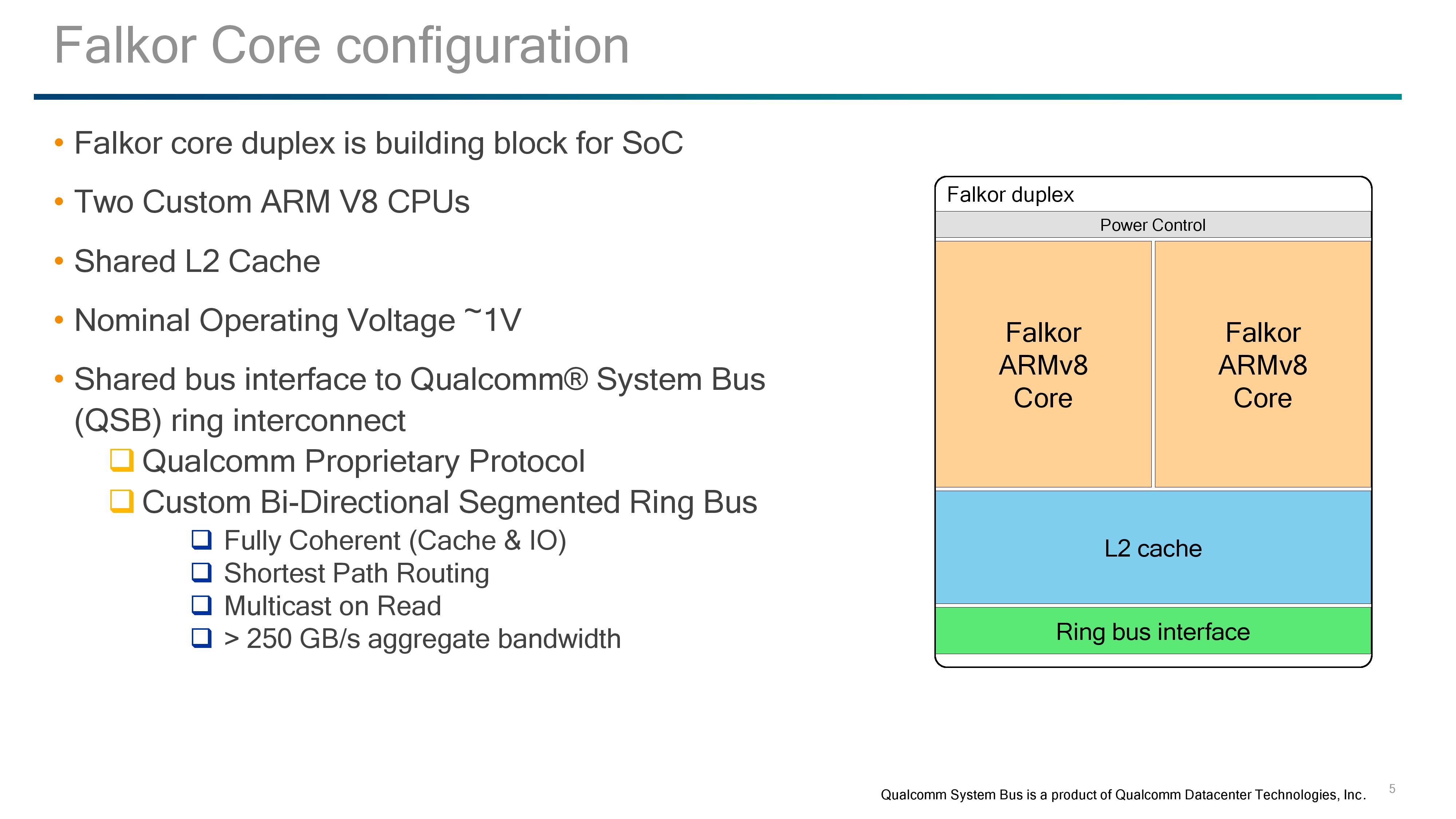
For SoC design followers, one might look at this design and think they see similarities with other dual-core designs such as AMD’s original Bulldozer design from 2011 or Intel's Xeon Phi. Internally, the cores are completely separate in terms of instruction throughput with no shared resources before the L2 cache. Consequently, between the two ends of the spectrum, Falkor is much closer to a Xeon Phi dual-core module, where each core has its own set of execution ports and vector extensions, but share an L2 cache and network connectivity.
But before diving into the cores, the L2 cache and power control require some explaining.
The L2 cache is a unified cache between both cores with ECC support, and inclusive of the L1-Data caches on both. Accesses are 128-byte interleaved with 128-byte lines, with 32-bytes per direction per interleave per cycle and 8-way associativity. ECC is using SEC-DED methodology, and the overall result as a minimum 15 cycle latency for an L2 hit, which is very competitive in the market. Qualcomm isn’t stating the size of the L2 cache at this time, which is somewhat of a surprise. In the market we see a variety of L2 cache options, so Qualcomm might end up offering a series of processors with different amounts of L2, especially if L2 defects are a factor in the manufacturing.

For power control, Qualcomm uses this unified design to control both cores. During our briefing we were told that both cores have to share the same frequency for L2 consistency; however the voltage per core can be adjusted and optimized for the best power implementation. As a result, power states between the cores can vary, and depending on the workflow needed, the cores and the L2 can also have different power states.
The cores in the duplex are powered by a block head switch or a low-dropout regulator (LDO), depending on the requirement. This allows for a variety of power down modes for the core logic, registers and caches:
- Light Sleep: CPU Clock is gated/lowered
- Voltage Retention: Registers and Caches retain state, logic is effectively off
- Register Retention: Registers retail state using main chip power rail, caches are off
- Collapse: Registers and L1 state not retained
The power control also maintains the state of the L2 cache, which offers modes similar to the CPU and may clock gate completely even with the CPUs in use. We confirmed that the L2 cache can only be on or off, and not in a half-use state.
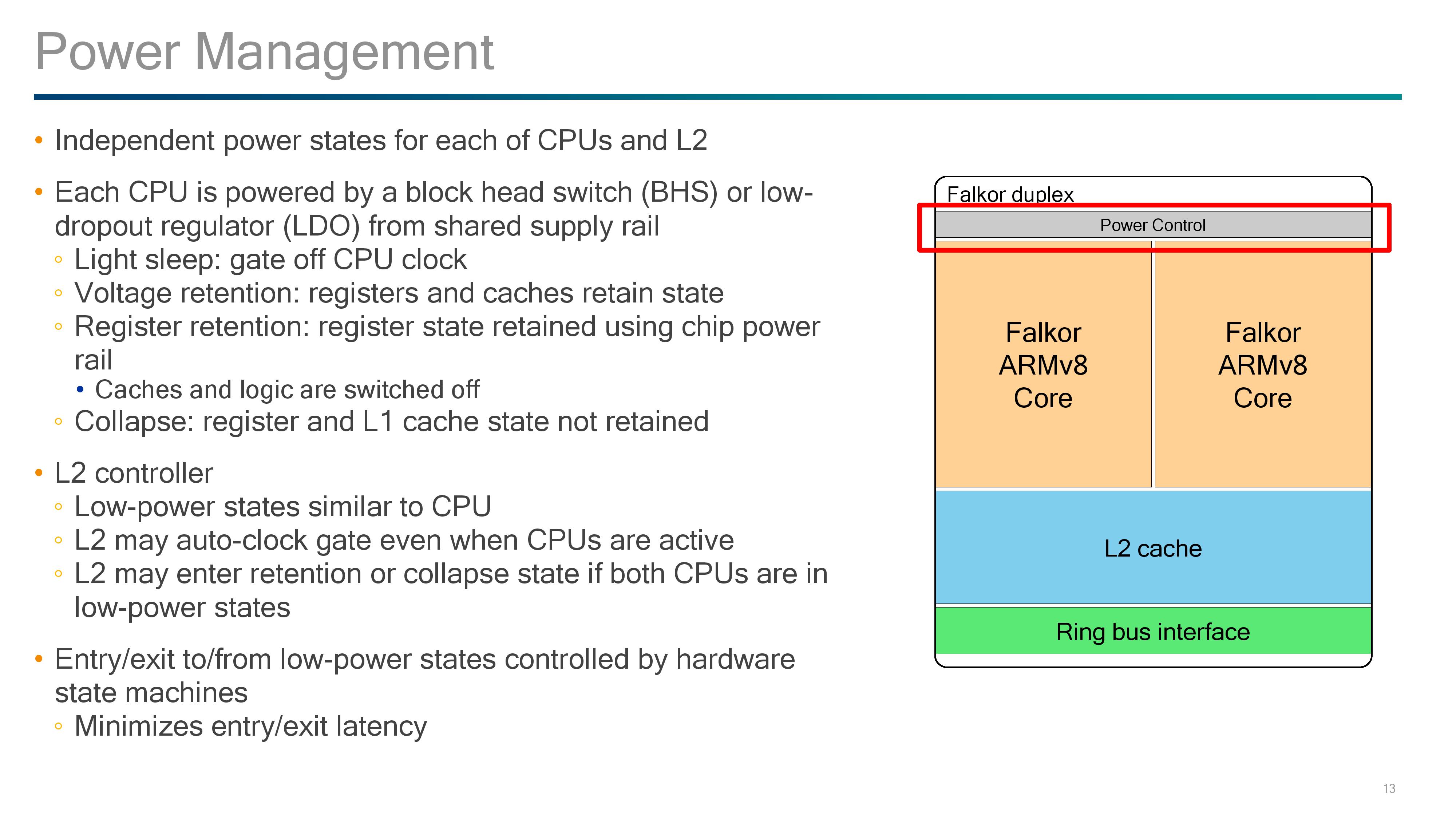
Overall for power, Qualcomm is also implementing hardware state machines, to enable quick entry and exit to and from low power modes. Qualcomm explained that CPU use in data centers can be super low depending on time of day and requirements, so the ability to save power wake quickly was a fundamental design aspect for this chip, with the aim of reducing the electricity bill.
We know that these chips are built on a 10nm process, and when questioned Qualcomm stated that they will run above 2.0 GHz, while talking in about 1.0 V to do so while also being competitive in performance per watt. Unfortunately requests regarding TDP were returned with 'competitive for a data center environment'.


41 Comments
View All Comments
SarahKerrigan - Sunday, August 20, 2017 - link
I seriously doubt SVE is present. As far as I know, Fujitsu is still lined up to be the first SVE user, and it's not like ultra-wide vectors are a massive boost to conventional enterprise servers.Kevin G - Sunday, August 20, 2017 - link
Using SVE requires ARM v8.2A support which this does not appear to have. The ARM v8.2A spec only was announced in January 2016, which isn't enough time to get it implemented into anything that'd be shipping now. Qualcomm could have been working behind the scenes but that would have given them perhaps another year with a spec that could change before formal publishing (i.e. may require some last minute changes right past the design would be tapping out). For a server part, that path would be unwise.SVE was announced a year ago and is far more complex than the v8.2A released due to how it handles execution width. A SVE design right now is a virtual impossibility.
Hurr Durr - Sunday, August 20, 2017 - link
I`d rather read something on x86 thing on ARM that MS and Qualcomm have than this. Much more potential for the real world.Kevin G - Sunday, August 20, 2017 - link
Can we get an editor in here?"For SoC design followers, one might look at this design and think they see similarities with designs such as AMD’s original Bulldozer design from 2011. ... Actually, after writing that last sentence, it is basically a Xeon Phi dual core module."
While perfectly readable, that last paragraph could use a bit of a rewrite due to the last sentence nullifying it. My quick stab at a rewrite:
For SoC followers, the Qualcomm pairs two modules per fabric stop similar to what Intel has implemented in their most recent Xeon Phi chips. Unlike the new grid topology in the Xeon Phi, Qualcomm is using a ring bus akin to what Intel uses on its Xeon E5 and E7 chips. Those thinking that a dual core module would follow AMD's Bulldozer philosophy will be disappointed to learn that no execution resources are shared between the cores, just the L2 cache, power management and bus interface.
The same comparisons and ideas are made but they flow to the reader a bit more logically to me.
FunBunny2 - Sunday, August 20, 2017 - link
-- Unlike the new grid topology in the Xeon Phi, Qualcomm is using a ring bus akin to what Intel uses on its Xeon E5 and E7 chips.I've long wondered how hardware engineers:
1) discover such alternatives
2) decide which one to choose
Is this fundamental math and physics laws, or trial and error? anyone know a readable (for the non-physics major, that is) source?
Kevin G - Monday, August 21, 2017 - link
Topology has been a well studied concept. At a high level, this mimics general networking design closely. The choice of on-die topology is generally at the mercy of engineering trade offs that are unique in this context.The ring bus you get an easy means of scaling the number of units but the trade of is an increase in latency around the ring bus as the numbers go up. Diminishing returns are hit as the numbers increases. With a ring though, individual units on the ring can be radically different sizes on a die as long the links between stops can be roughly the same for timing purposes. A ring bus also permits a relatively predictable latency to reach stops further away, something noteworthy for implementing coherency protocols. Another trade off with the ring design is that it'll always consume power. Nodes that are not in use still need to have the ring stop going to permit data passage through it.
Qualcomm side steps the ring issue a little bit by including two cores per ring stop, thus putting the minimum number of stops at 24. Just like Intel, I suspect on-die IO like PCIe, memory controllers etc. will have their own ring stops. It is not clear if this all on one massive ring bus or like the last generation of E5/E7 high core count chips, several rings are used with discrete bridges between them. Intel never went beyond 16 ring stops in a design.
A grid topology requires far greater engineering resources to implement correctly. Physical size has to be the same for those nodes in the middle of the grid but there is a bit of wiggle room along the perimeter to expand in one of the two dimensions (handy for things like PCIe, memory controllers that have a fixed need per socket). Cache coherency has to account for variable latency between nodes on the grid: there are several paths to between source and destination. The main benefit of a grid though is that scaling is vastly improved as core count increases. Another benefit is that not all the links in between cores needs to be active to move data. This saves power. Due to the ability to route around congested links, the individual links between grid nodes do not necessarily have to be as wide as those on a ring, saving a bit of energy there while maintaining similar aggregate bandwidth. For servers, multi-pathing of data (ie sending it twice) is also possible for increased RAS if an error in transmit is encountered along a particular path. Intel hasn't indicated that they're doing multipathing but could be a feature they add down the road. In the future if chips stacking emerges outside of research labs as feasible, the grid topology can also expand into the 3rd dimension.
The recent Xeon Phi isn't Intel's first attempt at a grid topology. The first publiclly shown off design was there Terascale research chip a decade ago. ( http://www.eetimes.com/document.asp?doc_id=1303295 ) Inter core topology was a major driver of that research effort and the recent Xeon Phi and Xeon series are the result of those efforts. Intel isn't event the first to implement a grid topology. The Compaq/DEC Alpha EV7 did so between sockets and permitted up to 64 sockets in an 8 x 8 grid from the early 2000's. IBM used a grid-like design for their BlueGene super computer designs to move data, though that wasn't cache coherent. There could be earlier instances as those are a few that I know off hand.
FunBunny2 - Monday, August 21, 2017 - link
thanks. much clearer.Ryan Smith - Sunday, August 20, 2017 - link
Thanks!Lord-Bryan - Sunday, August 20, 2017 - link
"So we have to admit that we were surprised by Qualcomm releasing so much information about the pipeline. When we’ve ever asked the mobile CPU team about Krait and Kryo, we usually hit a brick wall, left with a PR answer of a ‘custom core design’ or the guide of ‘protecting our design"Well am not surprised, releasing architectural details of server cpus, has always been an industry norm. It is something they just have to do if they want to be relevant, you can't just sell black boxes worth thousands of dollars to just anyone.
Lord-Bryan - Sunday, August 20, 2017 - link
Plus developers will have to know how the processor works in other to optimize applications for it, Qualcomm is playing with the big boys now, no room for unnecessary pride.