Analyzing Falkor’s Microarchitecture: A Deep Dive into Qualcomm’s Centriq 2400 for Windows Server and Linux
by Ian Cutress on August 20, 2017 11:00 AM EST- Posted in
- CPUs
- Qualcomm
- Enterprise
- SoCs
- Enterprise CPUs
- ARMv8
- Centriq
- Centriq 2400
The Duplex and Power Management
Like many processors on the market, design companies will use building blocks to assemble their complete processors. Equip those blocks with the right protocols, put them together, optimize, and create an advanced piece of sand that can decompress cat gifs if we prod it in the right way. Qualcomm’s main building block at the SoC level is the Falkor duplex, containing two Falkor cores, a shared L2 cache, QSB/fabric connectivity, and represents the lowest level of power management.
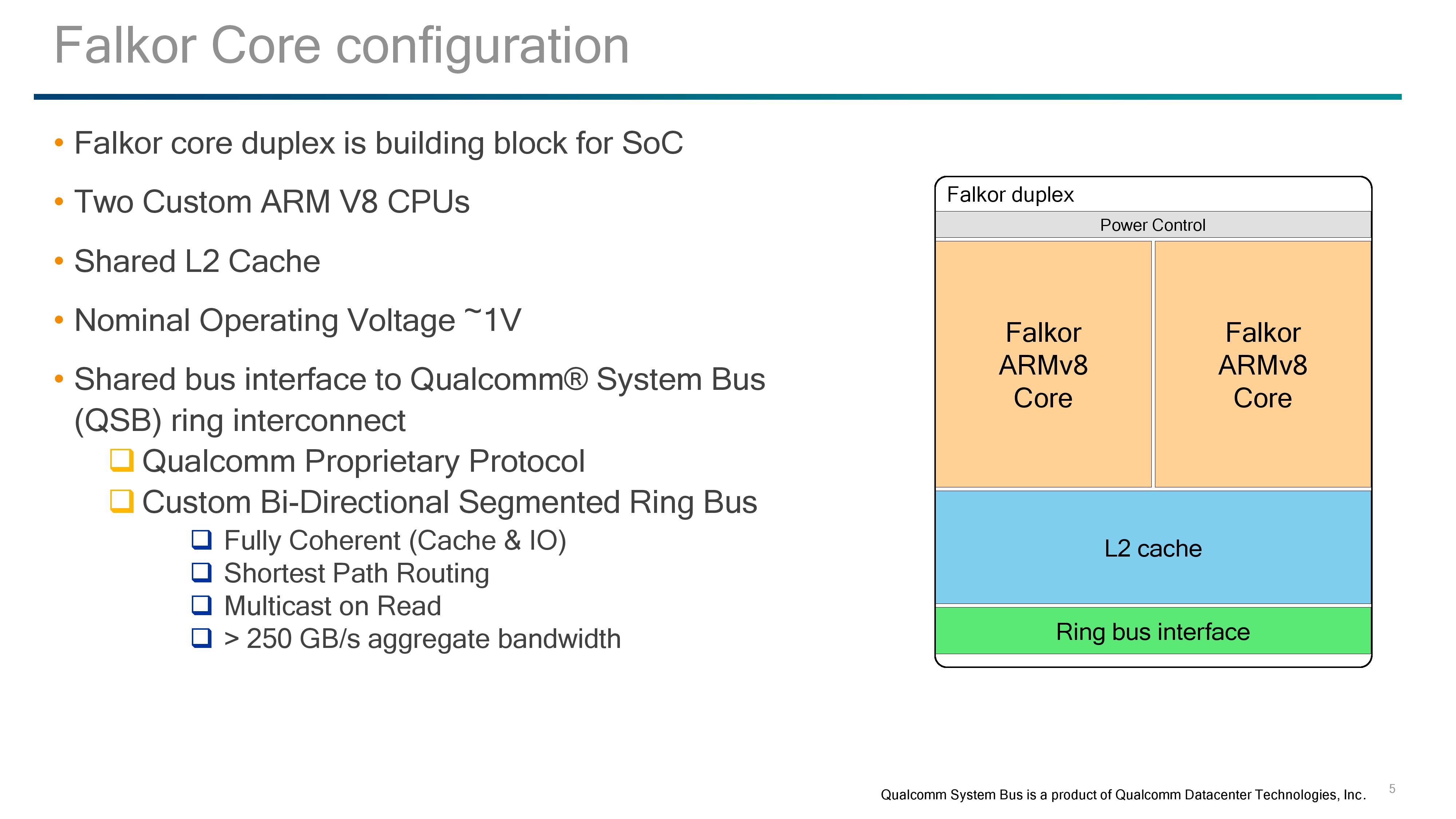
For SoC design followers, one might look at this design and think they see similarities with other dual-core designs such as AMD’s original Bulldozer design from 2011 or Intel's Xeon Phi. Internally, the cores are completely separate in terms of instruction throughput with no shared resources before the L2 cache. Consequently, between the two ends of the spectrum, Falkor is much closer to a Xeon Phi dual-core module, where each core has its own set of execution ports and vector extensions, but share an L2 cache and network connectivity.
But before diving into the cores, the L2 cache and power control require some explaining.
The L2 cache is a unified cache between both cores with ECC support, and inclusive of the L1-Data caches on both. Accesses are 128-byte interleaved with 128-byte lines, with 32-bytes per direction per interleave per cycle and 8-way associativity. ECC is using SEC-DED methodology, and the overall result as a minimum 15 cycle latency for an L2 hit, which is very competitive in the market. Qualcomm isn’t stating the size of the L2 cache at this time, which is somewhat of a surprise. In the market we see a variety of L2 cache options, so Qualcomm might end up offering a series of processors with different amounts of L2, especially if L2 defects are a factor in the manufacturing.

For power control, Qualcomm uses this unified design to control both cores. During our briefing we were told that both cores have to share the same frequency for L2 consistency; however the voltage per core can be adjusted and optimized for the best power implementation. As a result, power states between the cores can vary, and depending on the workflow needed, the cores and the L2 can also have different power states.
The cores in the duplex are powered by a block head switch or a low-dropout regulator (LDO), depending on the requirement. This allows for a variety of power down modes for the core logic, registers and caches:
- Light Sleep: CPU Clock is gated/lowered
- Voltage Retention: Registers and Caches retain state, logic is effectively off
- Register Retention: Registers retail state using main chip power rail, caches are off
- Collapse: Registers and L1 state not retained
The power control also maintains the state of the L2 cache, which offers modes similar to the CPU and may clock gate completely even with the CPUs in use. We confirmed that the L2 cache can only be on or off, and not in a half-use state.
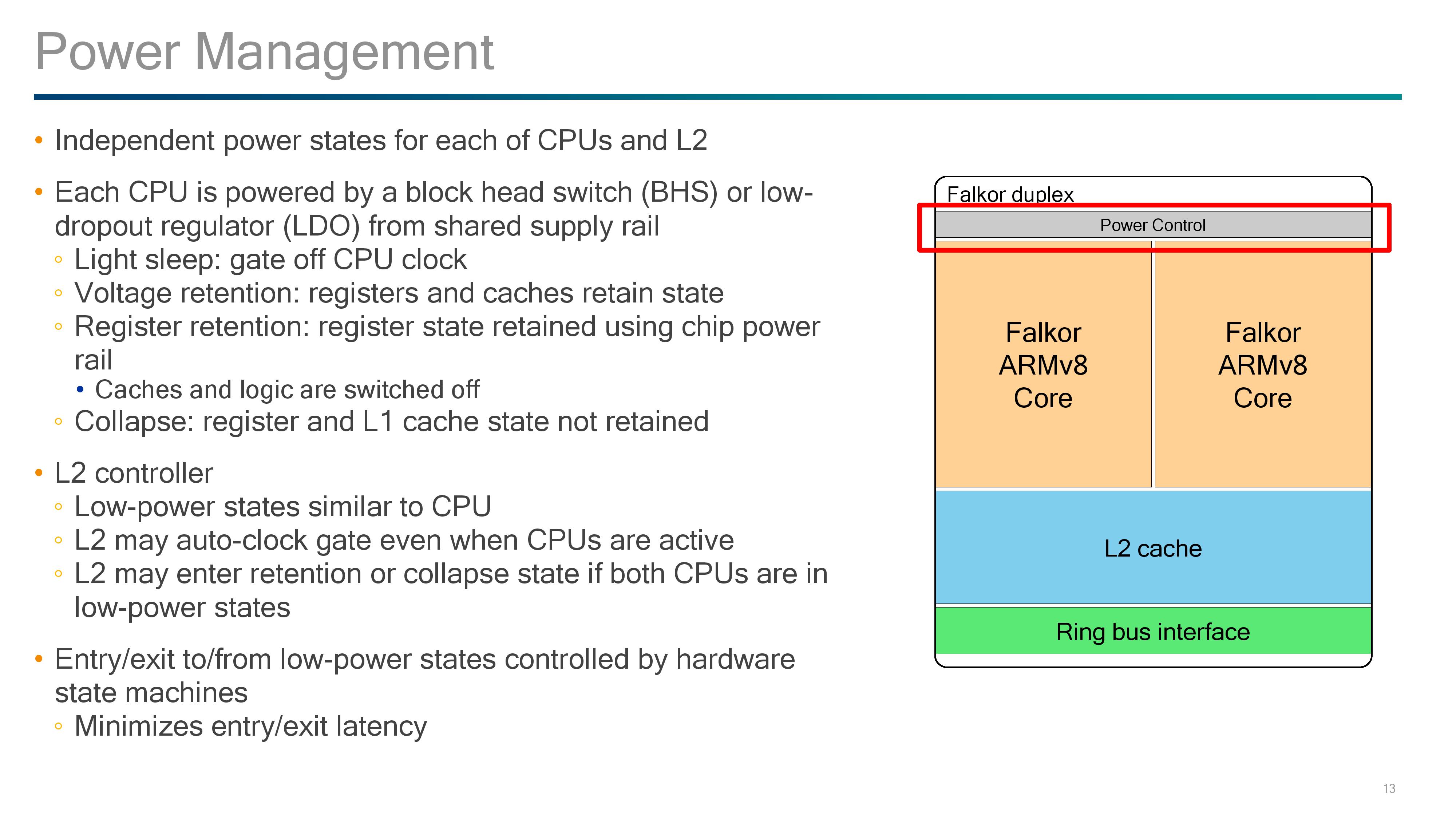
Overall for power, Qualcomm is also implementing hardware state machines, to enable quick entry and exit to and from low power modes. Qualcomm explained that CPU use in data centers can be super low depending on time of day and requirements, so the ability to save power wake quickly was a fundamental design aspect for this chip, with the aim of reducing the electricity bill.
We know that these chips are built on a 10nm process, and when questioned Qualcomm stated that they will run above 2.0 GHz, while talking in about 1.0 V to do so while also being competitive in performance per watt. Unfortunately requests regarding TDP were returned with 'competitive for a data center environment'.


41 Comments
View All Comments
SarahKerrigan - Sunday, August 20, 2017 - link
"Cavium is the most notable public player using ARM designs in commercial systems so far (there are a number of non-public players focusing on niche scenarios, or whom have little exposure outside of China). The latest design, the Cavium ThunderX2, uses the main A-series core licenses and interconnect license from ARM to provide large numbers of mobile-class CPU cores with as much memory bandwidth and IO as possible."This is not even remotely true. Neither Cavium's cores nor Cavium's interconnect (CCPI predates Cavium's jump to ARM) are ARM IP - they're using an architectural license, *not* IP blocks (or at least, not those ones.) ThunderX uses custom Cavium cores that are between A53 and A57 in performance, while ThunderX2 uses a small number of cores (32) based on the XLP/Vulcan design they bought from Broadcom.
To make that last part more confusing, Cavium initially announced a *different* ThunderX2, which was an enhanced (54-core) derivative of the original ThunderX design. This seems to have been killed when the Vulcan uarch was licensed, or at least has not been heard from since.
Ian Cutress - Sunday, August 20, 2017 - link
That's my fault, I wrote this while flying and thought I had known what is under the hood on ThunderX. Johan actually did a good write up on this, and I'll edit the piece here appropriately.http://www.anandtech.com/show/10353/investigating-...
SarahKerrigan - Sunday, August 20, 2017 - link
"uses the architecture licence for the main A-series core from ARM"That makes even less sense. A-series cores don't factor into it. ThunderX is custom.
name99 - Sunday, August 20, 2017 - link
Is this public knowledge (original ThunderX2 killed, new ThunderX2 based on Vulcan)?I know it's public that (beginning of this year) Cavium acquired Vulcan IP, but I'd not heard anything beyond that. ThunderX2 is supposed to ship Q3 this year (ie RSN...) which to me suggests they're too far along to drop it, and Vulcan will be the basis of ThunderX3.
SarahKerrigan - Sunday, August 20, 2017 - link
Yes. There have been a number of commits to LLVM, etc, indicating that ThunderX2 is now Vulcan. Cf the ThunderX2 LLVM model, which straight-up says "Based on Broadcom Vulcan."I don't know whether the original TX2 design is fully dead or merely mostly dead, but it's pretty obvious at this point that a Vulcan-based TX2 is coming.
SigismundBlack - Sunday, August 20, 2017 - link
Thanks for the info.Denverton rather than 'Denveron'.
Since the C3000 Atom series is cited here re it's also seems worth mentioning AMDs low power server SOCs (e.g. X3421) which likewise feature in recent Moonshot systems and home/SOHO servers.
jameskatt - Sunday, August 20, 2017 - link
The biggest problem I see is if Qualcomm is going to be devoting resources for this project for the long-term. Businesses require stability, predictability, and long-term support. Qualcomm's competitors have been in the business for decades and will be in the business for decades. Qualcomm can't prove they will be in the business for decades to come particularly if they make no money on it.Kevin G - Sunday, August 20, 2017 - link
Qualcomm has been around for awhile so there is stability there. They are new to the ARM server market though because, well after many false starts this market appears to finally be emerging. Even though Qualcomm is just launching this chip, it would be beneficial to them to discuss a roadmap to bring some long term stability to the scene.Wardrive86 - Sunday, August 20, 2017 - link
Surely Qualcomm is using SVE and not regular NEON units. I wish they would expose how wide the units are. I'm very excited they were so open about their architecture. Great write up Ian as well!Dmcq - Sunday, August 20, 2017 - link
I doubt it. SVE is a biggie and was only announced recently, I can't see that Qualcomm would bother risking trying to put it in their first server chip.