The AMD Radeon RX Vega 64 & RX Vega 56 Review: Vega Burning Bright
by Ryan Smith & Nate Oh on August 14, 2017 9:00 AM ESTSizing Up Today’s Launch: RX Vega 64 & RX Vega 56
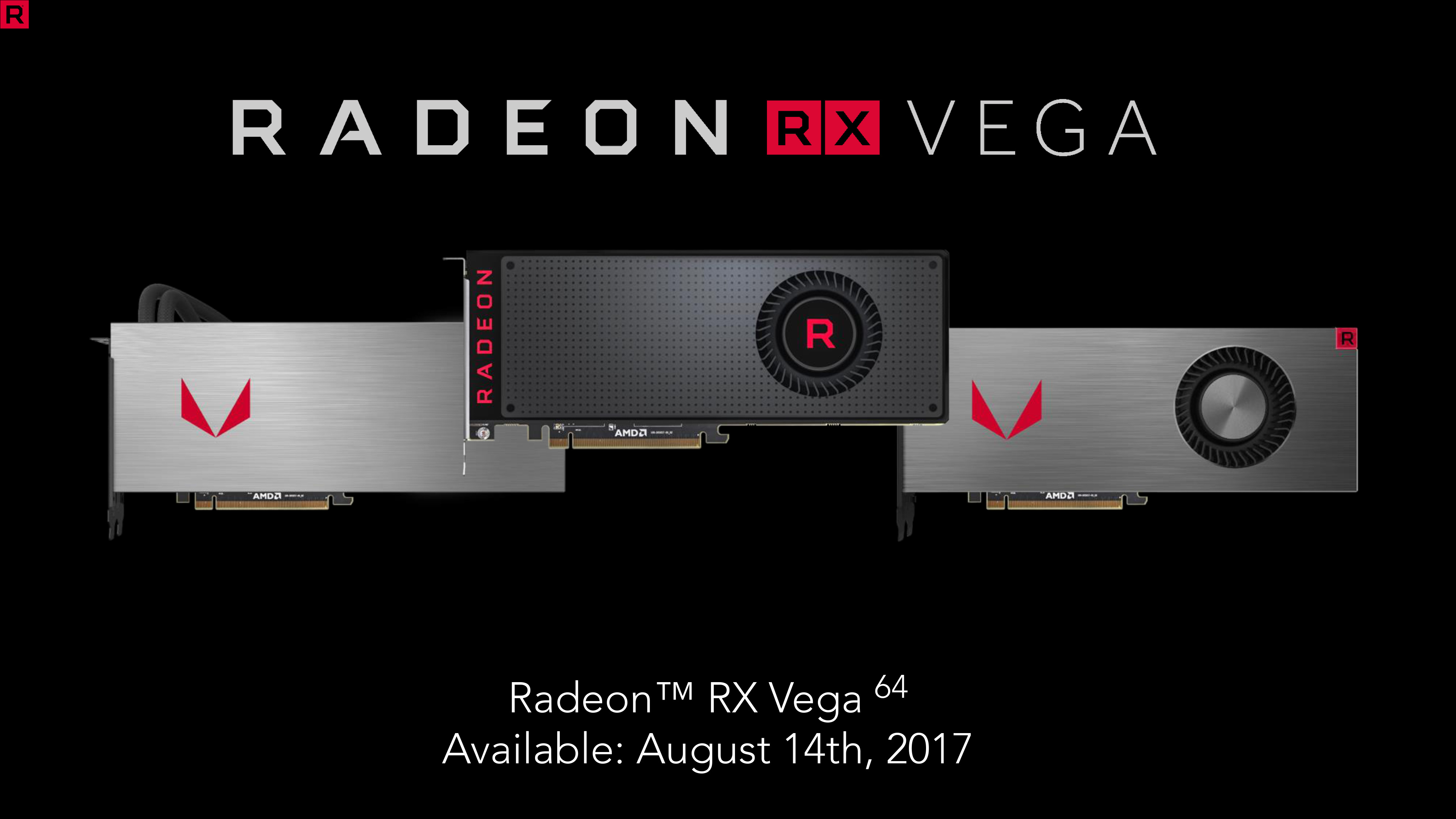
Now that we’ve gone through the architectural details of Vega, let’s size up today’s launch with the Radeon RX Vega 64 and Radeon RX Vega 56. While this isn’t quite a traditional one-two launch since Vega 56 doesn’t come out for another two weeks, it otherwise follows the usual pattern. That means a high-performance, fully-enabled card at the top, with its salvaged, lower-clocked, lower-priced counterpart below it.
| AMD Radeon RX Series Specification Comparison | ||||||
| AMD Radeon RX Vega 64 Liquid | AMD Radeon RX Vega 64 | AMD Radeon RX Vega 56 | AMD Radeon R9 Fury X | |||
| Stream Processors | 4096 (64 CUs) |
4096 (64 CUs) |
3584 (56 CUs) |
4096 (64 CUs) |
||
| Texture Units | 256 | 256 | 224 | 256 | ||
| ROPs | 64 | 64 | 64 | 64 | ||
| Base Clock | 1406MHz | 1247MHz | 1156MHz | N/A | ||
| Boost Clock | 1677MHz | 1546MHz | 1471MHz | 1050MHz | ||
| Memory Clock | 1.89Gbps HBM2 | 1.89Gbps HBM2 | 1.6Gbps HBM2 | 1Gbps HBM | ||
| Memory Bus Width | 2048-bit | 2048-bit | 2048-bit | 4096-bit | ||
| VRAM | 8GB | 8GB | 8GB | 4GB | ||
| Transistor Count | 12.5B | 12.5B | 12.5B | 8.9B | ||
| Board Power | 345W | 295W | 210W | 275W (Typical) |
||
| Manufacturing Process | GloFo 14nm | GloFo 14nm | GloFo 14nm | TSMC 28nm | ||
| Architecture | Vega (GCN 5) |
Vega (GCN 5) |
Vega (GCN 5) |
GCN 3 | ||
| GPU | Vega 10 | Vega 10 | Vega 10 | Fiji | ||
| Launch Date | 08/14/2017 | 08/14/2017 | 08/28/2017 | 06/24/2015 | ||
| Launch Price | $699* | $499/599* | $399/499* | $649 | ||
First off of course is the Radeon RX Vega 64. Based on a fully enabled Vega 10 GPU, this card is AMD’s best foot forward on Vega 10 performance. As it lives up to with its name, the Vega 64 ships with all 64 of Vega 10’s CUs enabled, giving the card 4096 SPs and 256 texture units. These CUs are in turn paired with AMD’s now L2 cache-backed ROPs, with a complete set of 64 of them.
In terms of clockspeed then, the Vega 64 can reach clockspeeds significantly higher than AMD’s Polaris cards, never mind the 28nm Fury X. In fact clockspeed is the single greatest resources AMD has for improving performance in existing games relative to Fury X, as while the architecture optimizations we talked about earlier do help performance in specific situations, nothing else has the raw potency and consistency of Vega’s much greater clockspeeds.
To this end the base clock is admittedly a bit low at 1247MHz, however the boost clock is at 1546MHz. As a reminder, AMD is taking a more NVIDIA-like stance with clockspeed advertising, so whereas Fury X’s boost clock was its highest attainable clockspeed (throttling when it couldn’t sustain it), RX Vega’s boost clock is the average clockspeed AMD expects the card to be able to sustain under gaming workloads. The card itself can actually boost even higher than this given a low-powered workload (e.g. something compute-heavy), with both of our sample cards boosting up to 1630MHz.
All told then, relative to its Fury X predecessor, on paper Vega 64 offers 47% higher shader, texture, geometry, and ROP throughput. These numbers don’t factor in Vega’s architecture enhancements, and in practice the actual performance gain will depend on what clockspeeds that the Vega 64 can attain, and conversely how much a given workload benefits from those aforementioned architectural improvements. So as with past architecture launches, the specs are only half of the story and the benchmarks will play the rest.

Paired with the Vega 10 GPU is 8GB of HBM2 memory, in the form of a pair of 4-Hi 4GB stacks. The two stacks are connected to Vega 10 via a 2048-bit wide memory bus running through the silicon interposer, and coupled with HBM2’s improved clockspeeds, gives Vega 10 GPU a lot of memory bandwidth in little space. AMD has clocked the memory at 1.89Gbps, giving the Vega 64 484GB/sec of memory bandwidth. With the original goal for the flagship card being a 2Gbps data rate (for a total of 512GB/sec) this does put Vega 64 at a slight disadvantage versus the previous Fury X. Which means that from an architectural perspective, AMD has to do more with slightly less.
Moving on, for better or worse the Vega 64 is a high-powered card in all senses of the word. AMD’s official board power specification for the card is 295W. Board power is a bit of a new metric for AMD; in previous generations they have published the typical board power of a card, whereas the 295W value here is no longer considered typical. Truthfully I don’t have a full grasp of the difference, but given our data and the fact that this value is higher than the Fury X’s typical board power of 275W, and this seems to function closer to a maximum for AMD. Which means that depending on the scenario a card can draw less than 295W, however as virtually all GPU-bound scenarios are also power-bound scenarios, it’s as good a number as any for a full load power specification.
For AMD, a high board power specification isn’t especially new. Fury X, Fury, and the R9 290X all shipped with high TBPs as well. But it means buyers should set their expectations accordingly for how the card will compare to past cards and the competition in terms of power consumption, and what acoustics might be like on this blower-based card.
Finally, while we’re not reviewing it today, AMD also has the RX Vega 64 Liquid Cooled edition. AMD is wisely not treating this card as the “baseline” performance of the Vega 64, but rather an enhanced enthusiast edition. This card has a boost clock rating of 1677MHz – 131Mhz above the air cooled card – and should perform a bit better than its non-liquid counterpart. However power consumption has more than gone up to match, with a 345W board power rating. This is going to be a low-volume halo part for enthusiasts who want the fastest Vega 64 possible, regardless of what it means for pricing or power consumption, and AMD is treating it accordingly.
Radeon RX Vega 56
Second on deck for today’s review embargo and arguably the focus of AMD’s promotional efforts is the Radeon RX Vega 56. The lower-tier counterpart to the RX Vega 64, the RX Vega 56 is the obligatory cut-down version of the RX Vega family. This features the same Vega 10 GPU as the Vega 64, however as accurately described in the name, only 56 of the 64 CUs are enabled on this card, leaving it with 3584 stream processors and 224 texture units.
Clockspeeds have also been cut down for the Vega 56, leading to the card shipping with a 1156MHz base clock and 1471MHz boost clock. On paper then, it offers 83% of the RX Vega 64’s compute and texturing performance, and 95% of the Vega 64’s ROP and geometry performance. Consequently, how the Vega 56 will perform in games has the potential to swing anywhere between a solid step below AMD’s flagship card, and something that gets a bit too close for comfort.
Meanwhile like its high-tier counterpart, the Vega 56 gets 8GB of HBM2 memory. Like its GPU clockspeed, memory clockspeeds have also been reduced to a less aggressive frequency here, leading to AMD shipping the card with a 1.6Gbps data rate. All told then, this gives the Vega 56 410GB/sec of memory bandwidth to work with, about 85% of Vega 64’s. Given that Vega 56’s compute/shading throughput is also about 85% of Vega 64’s, you can see how this memory configuration is a good match for Vega 56’s GPU configuration.
The upside of pulling back on performance is that AMD has also been able to pull back on power consumption. Vega 56 shaves 85W off of its board power rating, bringing it down to 210W. Which considering that on paper Vega 56 should deliver 85% of the performance of Vega 64, doing so at 71% of the power consumption looks very tantalizing in its own way.
The one catch specific to the Vega 56’s launch however is that it isn’t. Only the Vega 64 is launching today, while the Vega 56 will not be for sale until August 28th, making this a bit of a paper launch.


213 Comments
View All Comments
bcronce - Monday, August 14, 2017 - link
Exactly. I REALLY want to run my games in a VM guest.sutamatamasu - Monday, August 14, 2017 - link
In RTG slide on architecture side. Vega have some MB SRAM. Can you tell me what this SRAM use for?DanNeely - Monday, August 14, 2017 - link
Various caches and internal buffers; on die memory is normally SRAM because it's several times faster than DRAM. (DRAM is several times denser since it only uses 1 transistor/bit vs the 4(?) for SRAM; which is why its used for main memory where total capacity is more important - and where the data bus is the main latency source anyway.) I'd be curious what the breakdown is since only 4MB if it's in the L2 cache.sutamatamasu - Monday, August 14, 2017 - link
Yes, same with me. Like we all know GCN 5 has no change on L2 Cache size but i am curious, AMD say this SRAM and L2 Cache size differently.extide - Monday, August 14, 2017 - link
A lot of it is going to be in the low level L1 caches and stuff local to the shaders -- there are a lot of shaders, so it will add up fast. GCN 5 does have double L2 cache, at least according to this article, 4MB vs 2MB. AMD says there is a total of over 45MB of SRAM on there, which is pretty impressive for a GPU!ratbuddy - Monday, August 14, 2017 - link
I'm disappointed that Vega Frontier results were not included in the benches :-/Ryan Smith - Monday, August 14, 2017 - link
AMD did not sample that card, and there's not much of a reason for us to include it now when the RX Vega is faster.Nfarce - Monday, August 14, 2017 - link
Another Fury X fail. You'd have to be a hard core AMD fan to buy this over a GTX 1080, and that's not even taking into consideration the horrid power use compared to the 1080. Isn't that what AMD fans tell us is so important when comparing Ryzen to i7 CPUs in core/watt performance? Amazingly they are silent here.IchiOni - Monday, August 14, 2017 - link
I do not care about power consumption. Only poor people care about power consumption. I will be purchasing an air cooled Vega 64.Hurr Durr - Monday, August 14, 2017 - link
So Barnum was right in the end.