The AMD Radeon RX Vega 64 & RX Vega 56 Review: Vega Burning Bright
by Ryan Smith & Nate Oh on August 14, 2017 9:00 AM ESTVega 10: Fiji of the Stars
Before we dive into the Vega architecture itself, I want to start with the Vega 10 GPU proper, and as we look at its features you’ll soon understand why.
Vega 10 is for most practical purposes the successor to the Fiji GPU used in the Radeon R9 Fury and Nano products. And at face value this may seem a bit obvious – after all, it’s AMD’s first high-end GPU since then – but digging down a bit deeper, it’s interesting just how alike Fiji it is.
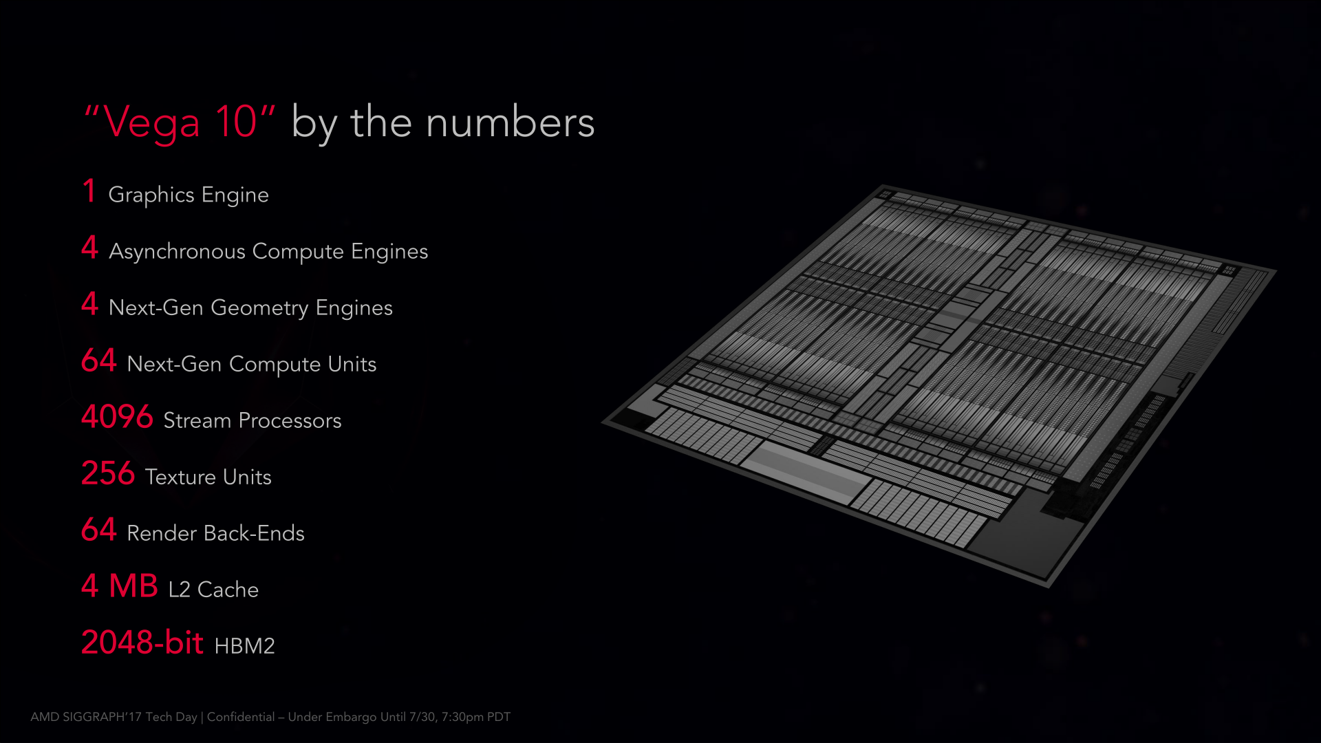
At a high level, Vega 10’s compute core is configured almost exactly like Fiji. This means we’re looking at 64 CUs spread out over 4 shader engines. Or as AMD is now calling them, compute engines. Each compute engine in turn is further allocated a portion of Vega 10’s graphics resources, amounting to one geometry engine and rasterizer bundle at the front end, and 16 ROPs (or rather 4 actual ROP units with a 4 pix/clock throughput rate) at the back end. Not assigned to any compute engine, but closely aligned with the compute engines is the command processor frontend, which like Fiji before it, is a single command processor paired with 4 ACEs and another 2 Hardware Schedulers.
On a brief aside, the number of compute engines has been an unexpectedly interesting point of discussion over the years. Back in 2013 we learned that the then-current iteration of GCN had a maximum compute engine count of 4, which AMD has stuck to ever since, including the new Vega 10. Which in turn has fostered discussions about scalability in AMD’s designs, and compute/texture-to-ROP ratios.
Talking to AMD’s engineers about the matter, they haven’t taken any steps with Vega to change this. They have made it clear that 4 compute engines is not a fundamental limitation – they know how to build a design with more engines – however to do so would require additional work. In other words, the usual engineering trade-offs apply, with AMD’s engineers focusing on addressing things like HBCC and rasterization as opposed to doing the replumbing necessary for additional compute engines in Vega 10.
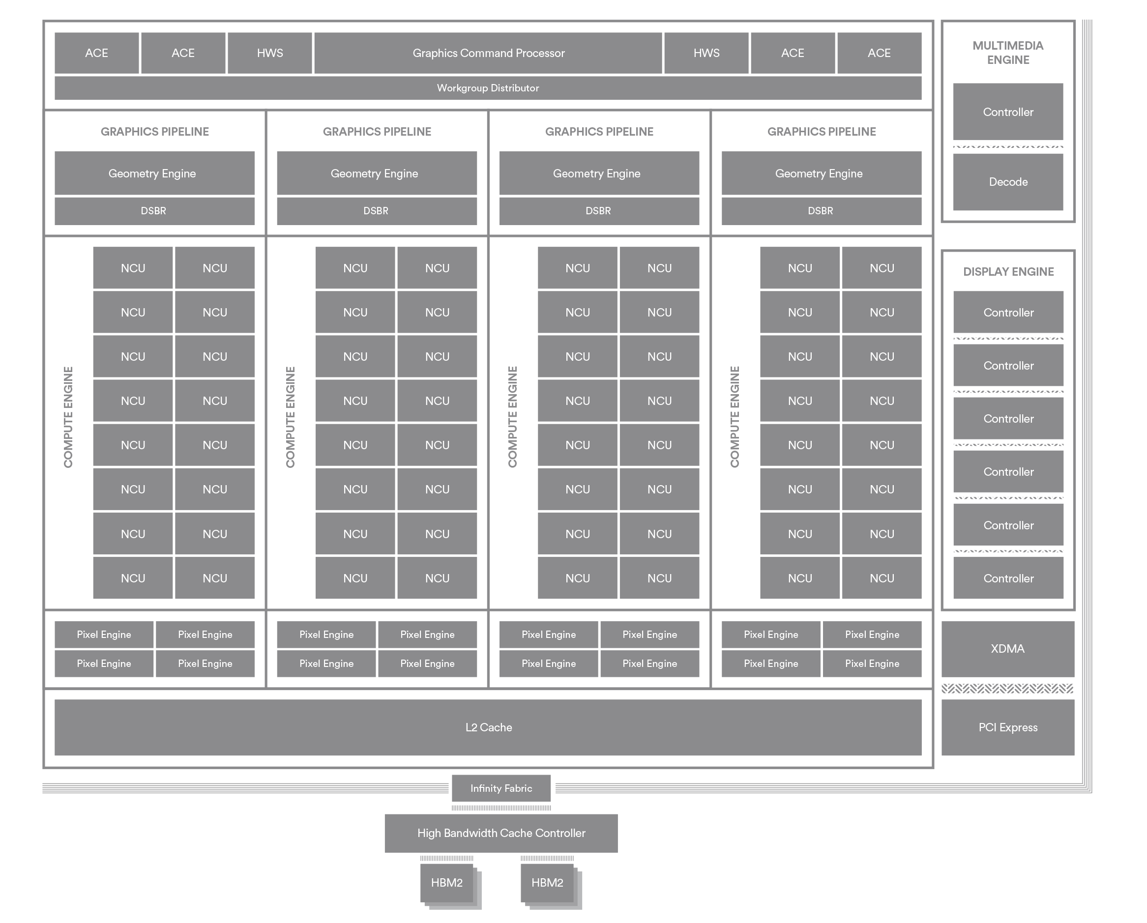
Not shown on AMD’s diagram, but confirmed in the specifications, is how the CUs are clustered together within a compute engine. On all iterations of GCN, AMD has bundled CUs together in a shader array, with up to 4 CUs sharing a single L1 instruction cache and a constant cache. For Vega 10, that granularity has gone up a bit, and now only 3 CUs share any one of these cache sets. As a result there are now 6 CU arrays per compute engine, up from 4 on Fiji.
It’s only once we get away from Vega 10’s compute core that we finally start to see some greater differences from Fiji. Besides being rewired to backstop the ROPs, the L2 cache has also been enlarged from 2MB on Fiji to 4MB on Vega 10. This growth not only gives Vega 10's L2 cache the room to serve the ROPs, but follows a general trend of ever-increasing cache sizes in GPUs.
But easily the biggest shift here is that AMD has moved from HBM to HBM2, and as a result they’ve halved the number of memory controllers from 4 to 2. As we’ll see in the card specifications, this costs Vega 10 just a bit of memory bandwidth since HBM2 hasn’t reached its intended speeds, but it saves AMD some die space, not to mention cuts down on the number of signal lines that need to be run off of the die and onto the silicon interposer
Connecting the memory controllers to the rest of the GPU – and the various fixed function blocks as well – is AMD’s Infinity Fabric. The company’s home-grown technology for low-latency/low-power/high-bandwidth connections, this replaces Fiji’s unnamed interconnect method. Using the Infinity Fabric on Vega 10 is part of AMD’s efforts to develop a solid fabric and then use it across the company; we’ve already seen IF in use on Ryzen and Threadripper, and overall it’s a lot more visible in AMD’s CPUs than their GPUs. But it’s there, tying everything together.
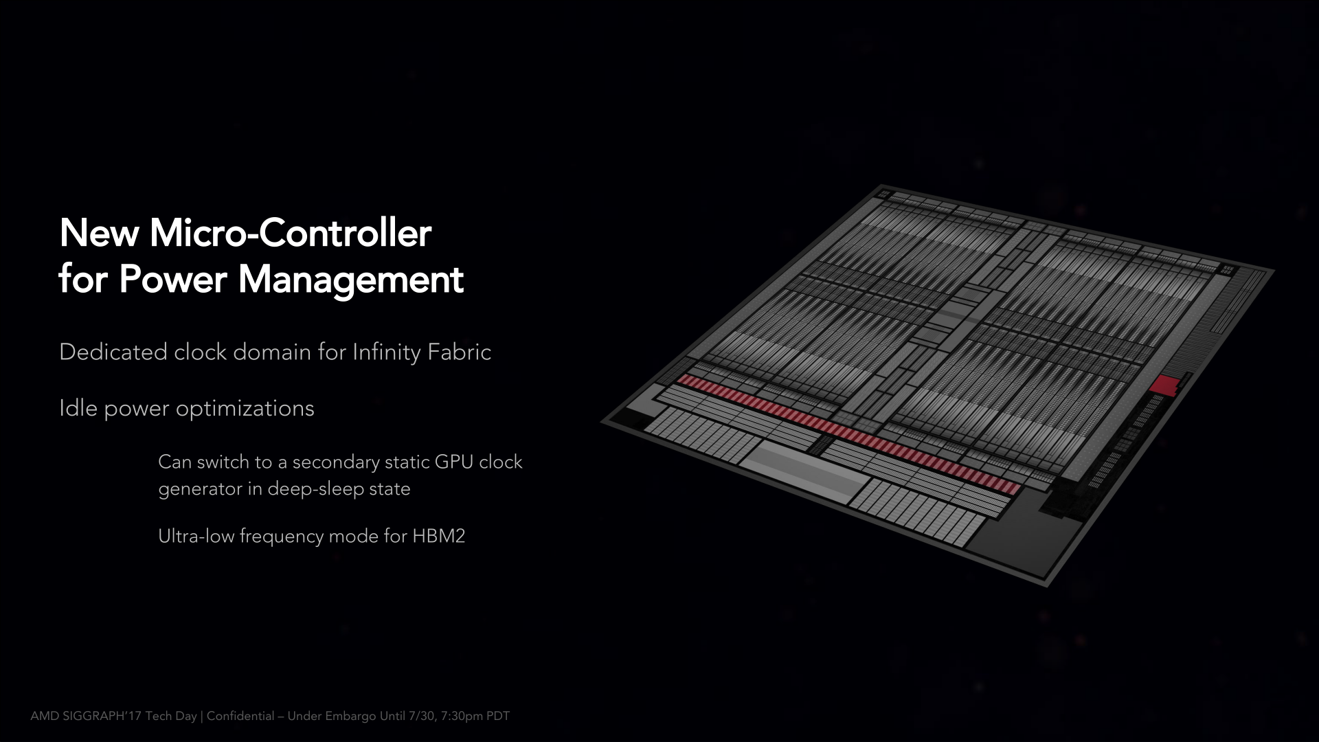
On a related note, the Infinity Fabric on Vega 10 runs on its own clock domain. It’s tied to neither the GPU clock domain nor the memory clock domain. As a result, it’s not entirely clear how memory overclocking will fare on Vega 10. On AMD’s CPUs a faster IF is needed to carry overclocked memory. But since Vega 10’s IF connects a whole lot of other blocks – and outright adjust the IF’s clockspeed based on the workload need (e.g. video transcoding requires a fast VCE to PCIe link), it’s not as straightforward as just overclocking the HBM2. Though similarly, HBM1 overclocking wasn’t very straightforward either, so Vega 10 is not a great improvement in this regard.
Otherwise, while all of the various fixed function units and engines have been updated over Fiji, their roles remain unchanged. So the multimedia engine, display engine, and XDMA engine are still present and accounted for.
Meanwhile it’s interesting to note that while Vega 10 is a replacement for Fiji, it is not a complete replacement for Hawaii. 2013’s Hawaii GPU was the last AMD GPU to be designed for HPC duties. Which is to say that it featured high FP64 performance (1/2 the FP32 rate) and ECC was available on the GPU’s internal pathways, offering a high reliability mode from GPU to DRAM and back again. Vega 10, on the other hand only offers the same 1/16th FP64 rate found on all other recent AMD GPUs, and similarly doesn’t have internal ECC. Vega 10 does do better than Fiji in one regard though, and that’s that it has “free” ECC, since the feature is built into the HBM2 memory that AMD uses. So while it doesn’t offer end-to-end ECC, it does offer it within the more volatile memory. Which for AMD’s consumer, professional, and deep learning needs, is satisfactory.

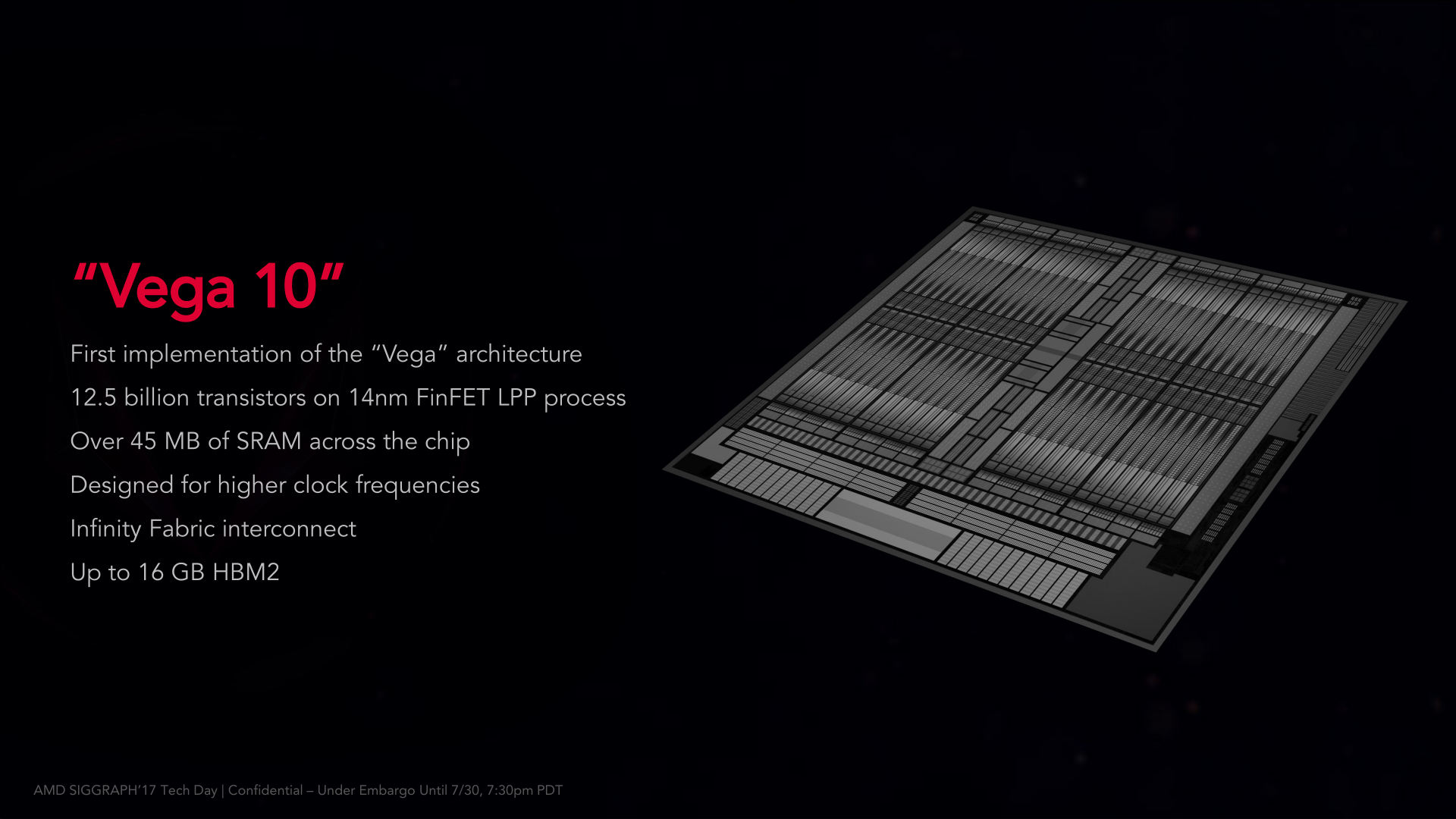
All told then, Vega 10 measures in at 486mm2 (ed: a nice number if I ever saw one), and like Polaris and the Ryzen CPUs, it’s built on partner GlobalFoundries’ 14nm LPP process. Within AMD’s historical pantheon of GPUs, this makes it 48mm2 larger than Hawaii and 110mm2 smaller than the late-generation Fiji. AMD has been producing GPUs at GlobalFoundries for a while now, so in a sense this is a logical progression from Polaris 10. On the other hand as AMD’s first high-end chip for the 14nm generation, this is the biggest they’ve ever started at.
That space is put to good use however, as it contains a staggering 12.5 billion transistors. This is 3.9B more than Fiji, and still 500M more than NVIDIA’s GP102 GPU. So outside of NVIDIA’s dedicated compute GPUs, the GP100 and GV100, Vega 10 is now the largest consumer & professional GPU on the market.
Given the overall design similarities between Vega 10 and Fiji, this gives us a very rare opportunity to look at the cost of Vega’s architectural features in terms of transistors. Without additional functional units, the vast majority of the difference in transistor counts comes down to enabling new features.
Talking to AMD’s engineers, what especially surprised me is where the bulk of those transistors went; the single largest consumer of the additional 3.9B transistors was spent on designing the chip to clock much higher than Fiji. Vega 10 can reach 1.7GHz, whereas Fiji couldn’t do much more than 1.05GHz. Additional transistors are needed to add pipeline stages at various points or build in latency hiding mechanisms, as electrons can only move so far on a single (ever shortening) clock cycle; this is something we’ve seen in NVIDIA’s Pascal, not to mention countless CPU designs. Still, what it means is that those 3.9B transistors are serving a very important performance purpose: allowing AMD to clock the card high enough to see significant performance gains over Fiji.
Overall Vega 10 is a very important chip for AMD because it’s going to be pulling double (if not triple) duty for AMD. It’s their flagship consumer GPU, but it’s also their flagship professional GPU, and it’s their flagship server GPU. This goes for both deep learning (Vega Instinct) and potential other future server products, such as virtualization cards. As AMD likes to boast, they had to do it all with one chip rather than NVIDIA’s hyper-segmented stack. Of course the reality is that AMD doesn’t have the resources to mirror NVIDIA’s efforts 1-to-1, so it means they have to be smarter about what they do in order to make the most of Vega 10.
Vega 10 won’t be alone however. As early as last year AMD reps confirmed that there’s a Vega 11 in the works, though at this time AMD isn’t saying anything about the chip. Given that Vega 10 is already a fairly large chip, and that Polaris chips decreased in size with their number, I’d expect Vega 11 to be a smaller version of Vega. Though where that fits into the Vega 10/Polaris 10 stack is anyone’s guess at this point.


213 Comments
View All Comments
bcronce - Monday, August 14, 2017 - link
Exactly. I REALLY want to run my games in a VM guest.sutamatamasu - Monday, August 14, 2017 - link
In RTG slide on architecture side. Vega have some MB SRAM. Can you tell me what this SRAM use for?DanNeely - Monday, August 14, 2017 - link
Various caches and internal buffers; on die memory is normally SRAM because it's several times faster than DRAM. (DRAM is several times denser since it only uses 1 transistor/bit vs the 4(?) for SRAM; which is why its used for main memory where total capacity is more important - and where the data bus is the main latency source anyway.) I'd be curious what the breakdown is since only 4MB if it's in the L2 cache.sutamatamasu - Monday, August 14, 2017 - link
Yes, same with me. Like we all know GCN 5 has no change on L2 Cache size but i am curious, AMD say this SRAM and L2 Cache size differently.extide - Monday, August 14, 2017 - link
A lot of it is going to be in the low level L1 caches and stuff local to the shaders -- there are a lot of shaders, so it will add up fast. GCN 5 does have double L2 cache, at least according to this article, 4MB vs 2MB. AMD says there is a total of over 45MB of SRAM on there, which is pretty impressive for a GPU!ratbuddy - Monday, August 14, 2017 - link
I'm disappointed that Vega Frontier results were not included in the benches :-/Ryan Smith - Monday, August 14, 2017 - link
AMD did not sample that card, and there's not much of a reason for us to include it now when the RX Vega is faster.Nfarce - Monday, August 14, 2017 - link
Another Fury X fail. You'd have to be a hard core AMD fan to buy this over a GTX 1080, and that's not even taking into consideration the horrid power use compared to the 1080. Isn't that what AMD fans tell us is so important when comparing Ryzen to i7 CPUs in core/watt performance? Amazingly they are silent here.IchiOni - Monday, August 14, 2017 - link
I do not care about power consumption. Only poor people care about power consumption. I will be purchasing an air cooled Vega 64.Hurr Durr - Monday, August 14, 2017 - link
So Barnum was right in the end.