Samsung Increases Production Volumes of 8 GB HBM2 Chips Due to Growing Demand
by Anton Shilov on July 19, 2017 8:00 AM EST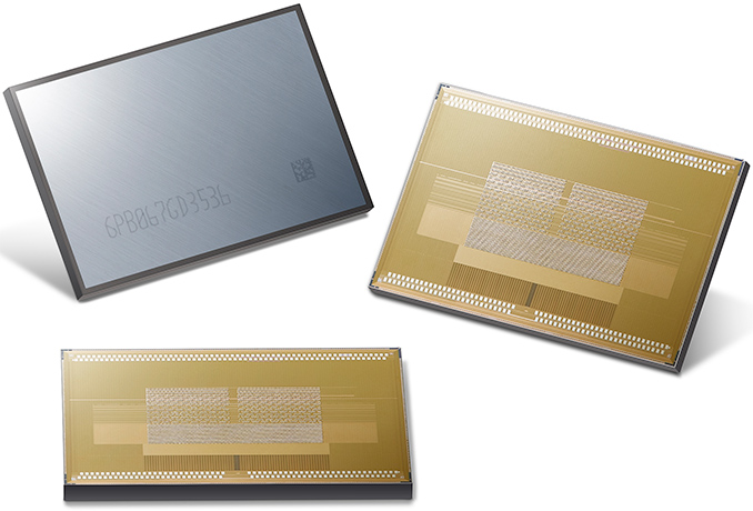
Samsung on Tuesday announced that it is increasing production volumes of its 8 GB, 8-Hi HBM2 DRAM stacks due to growing demand. In the coming months the company’s 8 GB HBM2 chips will be used for several applications, including those for consumers, professionals, AI, as well as for parallel computing. Meanwhile, AMD’s Radeon Vega graphics cards for professionals and gamers will likely be the largest consumers of HBM2 in terms of volume. And while AMD is traditionally a SK Hynix customer, the timing of this announcement with AMD's launches certainly suggests that AMD is likely a Samsung customer this round as well.
Samsung’s 8 GB HBM Gen 2 memory KGSDs (known good stacked die) are based on eight 8-Gb DRAM devices in an 8-Hi stack configuration. The memory components are interconnected using TSVs and feature over 5,000 TSV interconnects each. Every KGSD has a 1024-bit bus and offers up to 2 Gbps data rate per pin, thus providing up to 256 GB/s of memory bandwidth per single 8-Hi stack. The company did not disclose power consumption and heat dissipation of its HBM memory components.
Update 7/20: Samsung confirmed that the DRAM devices are made using 20 nm process technology, but could not disclose power consumption and TDP of KGSDs.
Samsung began mass production of 4-Hi HBM2 KGSDs with 4 GB capacity and 2 Gbps data rate per pin in early 2016. These chips have been used to build various solutions based on NVIDIA’s GP100 and later GV100 GPUs aimed at HPC and similar applications. The company also started to manufacture HBM2 KGSDs with 8 GB capacity in 2016 and so far, Samsung is the only company to publicly announce that they can mass-produce 8 GB HBM2 KGSDs.

Recently AMD launched its Radeon Vega Frontier Edition cards, the first commercial products featuring Vega and 8-Hi HBM2 stacks. To date we haven't been able to get confirmation of whose HBM2 AMD is using – frequent collaborator SK Hynix's or Samsung’s – however as Samsung is for now the only vendor to announce 8-Hi volume production, it's looking increasingly likely that AMD is using Samsung's HBM2. Meanwhile in the coming months AMD will expand the lineup of its graphics cards based on the Vega GPU with the RX Vega line for gamers, and considering that such devices are sold in mass quantities, Samsung has a very good reason for increasing HBM2 production..
Samsung expects 8 GB HBM2 KGSDs to account for over 50% of its HBM2 production by the first half of 2018.


Related Reading:
Source: Samsung


33 Comments
View All Comments
nathanddrews - Wednesday, July 19, 2017 - link
I'm not sure I could be more objective, actually. GDDR5X easily hits 480GB/sec bandwidth, which matches Vega FE. GDDR6 GPUs are expected to hit around 768GB/sec. HBM is awesome on paper, but so far we've only seen it used twice in consumer/prosumer cards and twice in deepwhatever cards. It seems pretty obvious that GPU processing power is not yet advanced enough to use that much bandwidth effectively. That's why I asked about multi-die GPUs, which could theoretically offer the performance of SLI/CF, but be seen as a single GPU.1. Fury (512GB/sec), GDDR5-equipped 980Ti, 1070, 1080, and 1080Ti, TitanXP/p beat it in games.
2. Vega FE (484GB/sec), GDDR5-equipped 1080 and 1080Ti, TitanXP/p beat it in games.
3. Tesla P100 (732GB/sec) and Instinct MI25 (484GB/sec), both irrelevant for games.
I'm sure HBM will be worthwhile eventually, but it's not anything special at the moment.
WinterCharm - Wednesday, July 19, 2017 - link
AMD's next generation GPU, Navi, is supposed to be scaleable. When you think about the Infinity Fabric and how Navi will work, it begins to make sense why AMD is going with HBM in Vega. Navi will be built on top of a more efficient version of Vega with multiple small dies and multiple stacks of HBM.Nvidia has already maxed out what TMSC can do in terms of die size with Volta V100... the modular GPU, much like Ryzen was the modular CPU, is the next logical progression.
nathanddrews - Wednesday, July 19, 2017 - link
Bingo. I'm excited to see where we go with scalable GPUs. Assuming they don't encounter any significant latency problems like with see with operations spanning CCX/NUMA, it should be super effective at maintaining generational leaps in performance for several more years.extide - Wednesday, July 19, 2017 - link
It's funny -- 3dfx was doing both multi-die GPU's and multi card setups, with NO issues in any game decades ago. Of course they ran glide and ancient versions of directx which were much simpler -- but still -- the fact remains. Voodoo 1 was a 2 chip GPU, and Voodoo 2 was a 3 chip GPU, and of course 3dfx invented SLI (of course the acronym stood for scan line interleave instead of scalable link interface back then). Too bad they never really innovated beyond the Voodoo2 -- the voodoo 3 was basically a Voodoo 2 on a single chip with a minor clock speed bump, and the Voodoo 4/5 ran on the VSA 100 chips which were basically a Voodoo 3 with again a bit of a clock bump, and then the Voodoo 5 ran two of them. I miss my Voodoo 5 -- I wish I still had it -- I traded it to someone for a Geforce 3, which while it was faster, it definitely doent have the same sort of nostalgia.nathanddrews - Wednesday, July 19, 2017 - link
LOL @ "NO issues in any game decades ago". I'm sorry, but Voodoo SLI only worked with a few games and was not free of issues.Also, it was not a "two chip" GPU in the sense we're talking about here. 3dfx had separate "chips" for each function of the overall GPU (TMU, frame buffer, etc.), not multiple wholly complete GPU dies on the same card.
James S - Wednesday, July 19, 2017 - link
They were multi-die but the 2nd and 3rd dies were TMU's (texturing unit) only so its a bit apple to oranges to what Navi will be. I wish they hung around, would be lovely having three major GPU vendors.CaedenV - Wednesday, July 19, 2017 - link
Um... history beautiful in hindsight? My memories of 3DFX GPUs were not quite a rosey. Constant driver and game compatibility issues, largely due to their multi-chip nature. Still, awesome cards... but without issue? hardly. Things are far FAR better today.James S - Wednesday, July 19, 2017 - link
Agree. The move to HBM is forward thinking as they really don't need the bandwidth for Vega but since AMD is a small company they are going to build Navi from Vega then it makes total since.sonicmerlin - Tuesday, July 25, 2017 - link
Pretty sure AMD is going with HBM because they're desperate to save some power with their power hungry GPUs.Manch - Wednesday, July 19, 2017 - link
HBM has been to include HBM1 very impressive. Even if you look at the older cards like the Fury with its 4Gb limit, The bandwidth allowed for some gains that enabled AMD to not be so far behind. The reduction in power alone allowed AMD to overvolt and drive the GPU faster. Granted it wasn't enough to beat NVidia cards but impressive none the less. The take away from HBM is same/more bandwidth for a lot less power. And that's already been shown within the limited power envelope of a gpu, the ability to redirect that powersavings to clock speed makes a difference between being way behind to only 90-95%.And don't compare VEGA FE yet. It's not a gamer card. Once Vega consumer GPU's drop. If the FE's are similarly performant then by all means rip them up.