AMD’s Radeon Vega Frontier Edition Formally Launches: Air Cooled For $999, Liquid Cooled for $1499
by Ryan Smith on June 27, 2017 11:50 AM EST- Posted in
- GPUs
- AMD
- Radeon
- Vega
- Vega Frontier Edition
After what appears to be a very unusual false start, AMD has now formally launched their new Radeon Vega Frontier Edition card. First announced back in mid-May, the unusual card, which AMD is all but going out of their way to dissuade their usual consumer base from buying, will be available today for $999. Meanwhile its liquid cooled counterpart, which was also announced at the time, will be available later on in Q3 for $1499.
Interestingly, both of these official prices are some $200-$300 below the prices first listed by SabrePC two weeks ago in the false start. To date AMD hasn’t commented on what happened there, however it’s worth noting that SabrePC is as of press time still listing the cards for their previous prices, with both cards reporting as being in-stock.
| AMD Workstation Card Specification Comparison | ||||||
| Radeon Vega Frontier Edition | Radeon Pro Duo (Polaris) | Radeon Pro WX 7100 | Radeon Fury X | |||
| Stream Processors | 4096 | 2 x 2304 | 2304 | 4096 | ||
| Texture Units | ? | 2 x 144 | 144 | 256 | ||
| ROPs | 64 | 2 x 32 | 32 | 64 | ||
| Base/Typical Clock | 1382MHz | N/A | N/A | N/A | ||
| Peak/Boost Clock | 1600MHz | 1243MHz | 1243MHz | 1050MHz | ||
| Single Precision | 13.1 TFLOPS | 11.5 TFLOPS | 5.7 TFLOPS | 8.6 TFLOPS | ||
| Half Precision | 26.2 TFLOPS | 11.5 TFLOPS | 5.7 TFLOPS | 8.6 TFLOPS | ||
| Memory Clock | 1.89Gbps HBM2 | 7Gbps GDDR5 | 7Gbps GDDR5 | 1Gbps HBM | ||
| Memory Bus Width | 2048-bit | 2 x 256-bit | 256-bit | 4096-bit | ||
| Memory Bandwidth | 483GB/sec | 2x 224GB/sec | 224GB/sec | 512GB/sec | ||
| VRAM | 16GB | 2 x 16GB | 8GB | 4GB | ||
| Typical Board Power | <300W | 250W | 130W | 275W | ||
| GPU | Vega (1) | Polaris 10 | Polaris 10 | Fiji | ||
| Architecture | Vega | Polaris | Polaris | GCN 1.2 | ||
| Manufacturing Process | GloFo 14nm | GloFo 14nm | GloFo 14nm | TSMC 28nm | ||
| Launch Date | 06/2017 | 05/2017 | 10/2016 | 06/24/15 | ||
| Launch Price | Air: $999 Liquid: 1499 |
$999 | $649 | $649 | ||
Meanwhile AMD has also posted the final specifications for the card, confirming the 1600MHz peak clock. Sustained performance is a bit lower, with AMD publishing a “Typical clock” of 1382MHz. It’s worth noting that this is the first time AMD has used this term – they’ve previously used the term “base clock”, which is generally treated as the minimum clockspeed a card under a full gaming workload should run at. AMD is typically very careful in their word choice (as any good Legal department would require), so I’m curious as to whether there’s any significance to this distinction. At first glance, “typical clock” sounds a lot like NVIDIA’s “boost clock”, which is to say that it will be interesting to see how often Vega FE can actually hit & hold its boost clock, and whether it falls below its typical clock at all.
Feeding the GPU is AMD’s previously announced dual stack HBM2 configuration, which is now confirmed to be a pair of 8 layer, 8GB “8-Hi” stacks. AMD has the Vega FE’s memory clocked at just under 1.9Gbps, which gives the card a total memory bandwidth of 483GB/sec. And for anyone paying close attention to AMD’s naming scheme here, they are officially calling this “HBC” memory – a callback to Vega’s High Bandwidth Cache design.

As for power consumption, AMD lists the card’s typical board power as “< 300W”. This is consistent with the earlier figures posted by retailers, and perhaps most importantly, this is AMD’s official typical board power, not the maximum board power. So we are looking at a fairly high TDP card, and given that AMD has had a great deal of time to sit and work on their reference blower designs over the last few years, I’m anxious to see what that means for this initial air-cooled card.
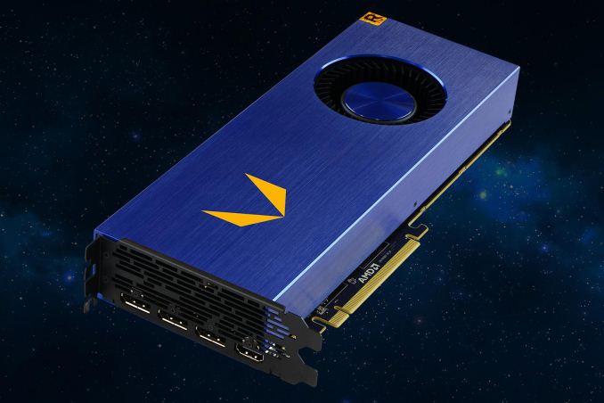
For display outputs, the Vega FE devotes its entire second slot to airflow, so all of the display connectors are found on the first slot. Typical for AMD cards of the past couple of years, we’re looking at 3x DP 1.4 ports along with 1x HDMI port. AMD is also throwing in a passive DP to SL-DVI adapter in the box.
Moving on, let’s talk about the software setup for the Vega FE. As this is a card meant for (in part) game developers, AMD has opted to give the card access to both their pro and gaming drivers. Taking things one step further however, rather than making them separate downloads and installations, AMD has merged both drivers into a single install. Users can now download a single driver package and simply switch between driver modes in AMD’s control panel, allowing quick access to both driver types.
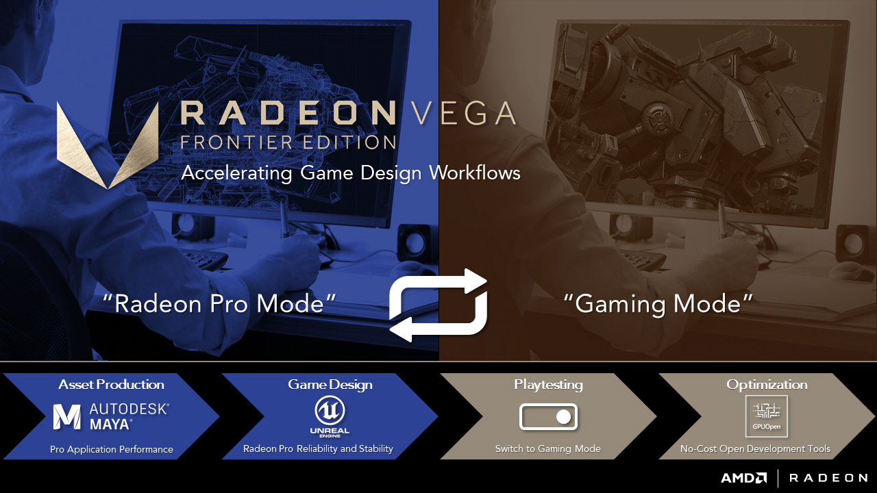
Unfortunately AMD hasn’t released much more in the way of detailed information on how driver switching works. In particular, it’s not clear whether switching requires a reboot or not; I would assume not, but it remains to be seen. Ultimately the primary purpose of this switch is for allowing game developers to switch modes for testing, going from pro driver mode for development to gaming mode for testing. The difference, I suspect, is less about driver code, and more about what driver optimizations are enabled. Games can get away with numerous hacks and optimizations in the name of performance, whereas professional applications need deterministic accuracy.
Otherwise, the driver situation touches on probably what remains one of the least-clear points of this product launch: who is the Radeon Vega Frontier Edition for? AMD is doing everything they can to encourage their typical Radeon consumer base to wait for the forthcoming Radeon Vega RX cards. In the meantime the company is stating that the card is “For Data Scientists, Immersion Engineers, and Product Designers” and certainly the pricing is closer to a professional card than a consumer card. Complicating matters is that AMD has been posting performance figures for SPECviewperf, Creo, other distinctly professional workloads, the kinds that typically go hand-in-hand with certified drivers. And at least for the moment, it doesn’t appear that AMD’s drivers have been certified (not that we’d expect them to be for a new architecture).
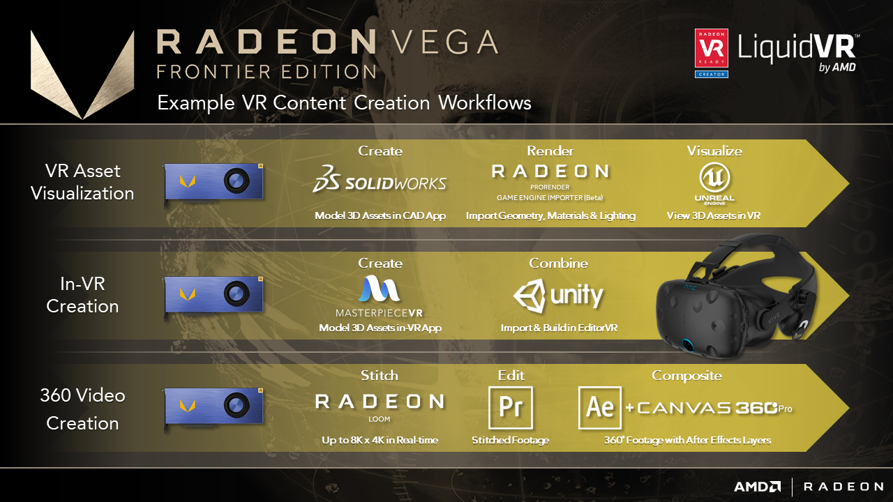
At a high level the Vega FE seems to compete with NVIDIA’s Titan Xp – and certainly that’s how AMD is choosing to pitch it – though this isn’t helped by the fact that NVIDIA isn’t doing a great job of establishing a clear market segmentation either, particularly since the launch of the GeForce GTX 1080 Ti. The Titan Xp is most certainly a partial gaming card (albeit a very expensive one), whereas AMD is focused more on professional visualization use cases that NVIDIA is not. Though where both overlap is on the compute front, where both the Vega FE and Titan Xp are essentially “entry-level” cards for production compute work. Otherwise, it may be better to treat the Vega FE as a beta testing card, especially given the “frontier” branding and the fact that AMD is clearly attempting to build out a more complete ecosystem for the future Vega RX and Instinct cards.
As for compute users in particular, AMD will be releasing the ROCm driver a bit later this week, on the 29th. Vega FE has a lot of potential for a compute card, thanks to its high number of SPs combined with equally high clocks. However serious compute users will need to code for its capabilities and idiosyncrasies to get the best possible performance on the card, which is all the more reason for AMD to get cards out now so that developers can get started. Compute will be the long-tail of the architecture: AMD can tweak the graphics performance of the card via drivers, but it's up to developers to unlock the full compute capabilities of the Vega architecture.
Wrapping things up, for anyone interested in picking up the Vega FE, AMD is currently only linking to Newegg’s storefront, where both the air cooled and water cooled cards are listed as “coming soon”. Otherwise SabrePC lists the cards in stock, albeit at prices over AMD’s MSRP.


Source: AMD


66 Comments
View All Comments
Yojimbo - Tuesday, June 27, 2017 - link
NVIDIA had been including 16 GB of HBM2 with 720 GB/s bandwidth for over a year, and they are just releasing a card with 900 GB/s bandwidth. The bandwidth limitations have more to do with cost control than the stacking topology of HBM versus HBM2.AMD chose to keep costs down and then subsequently chose to have more, slower VRAM rather than less, faster VRAM. With HBM1 having more than 4GB of VRAM was not a possibility, so such a choice was not available to AMD then. NVIDIA uses HBM2 on higher-priced cards and so can afford to have both large capacity and high bandwidth VRAM on them.
Stuka87 - Tuesday, June 27, 2017 - link
Yojimbo you are entirely wrong here. The GP100 shipped in March, not over a year ago. And it cost almost $9000, this is in NO WAY comparable to what AMD is offering here.nevcairiel - Tuesday, June 27, 2017 - link
Actually the Tesla P100 was available since around august 2016, so thats almost a year. Certainly its much more expensive, but that only underlines the argument that AMD choose the cheaper route to setup their HBM, going for capacity/price instead of bandwidth.CiccioB - Tuesday, June 27, 2017 - link
GP100 is in production since October 2015 and first samples used for internal server at Nvidia. The point is that HBM2 with that density and business width has been available for 18 months now.The use of just 2 stacks instead of 4 is for cost containment. The available bandwidth is not a technical constriction, just an economical one.
The fact that Nvidia can sell a similar card at 9 times the price of this one clearly indicates their different aims despite being similar in used resources and capabilities.
One has to wonder why AMD has to constantly discount their products to make them interesting to anyone wanting to use them.
Maybe HW, transistors, bandwidth and ALUs are not the only things that determine prices (though they determine costs, and in this case, very high costs).
I'm really interested in knowing what are the margins (or negative gains) for each Vega sold as a gaming card. Which is the reason I see for AMD to make the few of them, just to have benchmarks published, some extra positive comments but not real availability.
eek2121 - Tuesday, June 27, 2017 - link
You guys are confused. The first nvidia chip to use HBM2 was the P100 and it shipped in Q4 2016 in VERY limited quantities. There wasn't an HBM2 part prior to that as HBM2 WAS NOT AVAILABLE. Need sources? Try this very website for starters. Also, the Tesla P100 and beyond are NOT competitors to the Vega FE. They cost more than 10X as much for starters.CiccioB - Wednesday, June 28, 2017 - link
GP100 production started in October 2015. There are samples dated 43/2015 and they are not engineering samples. Since January 2016 produced Tesla cards where used to assemble a server in Nvidia (which appears on Top 500 faster HPC servers list) and in March 2016 Nvidia made available already assembled boards with P100 cards installed. Probably HBM2 was not available for anyone else, but Nvidia had its products done.For the comparison not being suitable due to the price, sorry, it's not how that works. Vega has been built with the same computing capabilities which are in GP100 (FP16, INT8, INT32 and fast with these even though less fast with FP64) . GP102 to which you want to compare has any of those capabilities. It's just that it arrived late, slower, more energy hungry and most of all without SW support.
That's why Vega can't be sold at Nvidia premium prices and margins.
Like Fiji, Vega arrived too late with too low performances. Good for patching the market segment for a while, at discounted price. Until Volta is released, after which even more discounted.
Being a generation behind does not help in selling at premium prices even though you build your GPU first the same work as the competition.
Yojimbo - Wednesday, June 28, 2017 - link
The P100 is the card we are talking about. You're wrong about when it first existed. The big internet companies were buying them up for internal use. Yes the card's volume grew as time went on, but it existed over a year ago.For the third time, the difference in price between the Tesla P100 and the Vega FE was my point. Despoiler said, "That's just the way HBM and HBM2 differ. HBM2 is more dense so it requires less stacks than HBM for a given capacity. Less stacks = more narrow bus = less bandwidth." But the P100 shows that it doesn't have to be that way. It is entirely technically possible for a card using HBM2 to have both 16GB of VRAM and bandwidth much higher than 483 GB/s.
AMD chose to use two 8-core-high stacks of HBM2 with 8 GB per stack for a 2048-bit bus and a total of 16 GB. They could have chosen to use four 4-high stacks of HBM2 with 4 GB per stack for a 4096-bit bus and the same total of 16 GB. They made the choice they did precisely because it's cheaper, not because the other choice is technically infeasible, unlike what Despoiler implied.
One more time for good measure: To make the bandwidth of the Vega FE lower than the bandwidth of the Fury X was a choice AMD made. It's not that it has to be that way because of the density of HBM2. Why is that so hard to understand?
CiccioB - Wednesday, June 28, 2017 - link
<blockquote>Why is that so hard to understand?</blockquote>Because fanboys need to address poor performances to undefined causes which have not to be related to AMD choices, skills or strategy. These ones are always perfect and it is the environment outside that is hostile for them to succeed.
Think about it. Whatever AMD problem, the cause is always by others.
T1beriu - Tuesday, June 27, 2017 - link
Flawed logic.DanNeely - Tuesday, June 27, 2017 - link
Half the stacks because twice as dense, unfortunately not quite twice as the clock speed so slightly less BW. Fewer stacks makes manufacturing easier because in makes the interposer somewhat simpler. NVidia's HBM 2 in Telsa cards is only running at 1.4/1.75GHz so I'm inclined to blame the HMB makers for not getting the clocks as high as were expected not AMD for having their memory controller fall short of design targets.