AMD's Future in Servers: New 7000-Series CPUs Launched and EPYC Analysis
by Ian Cutress on June 20, 2017 4:00 PM EST- Posted in
- CPUs
- AMD
- Enterprise CPUs
- EPYC
- Whitehaven
- 1P
- 2P
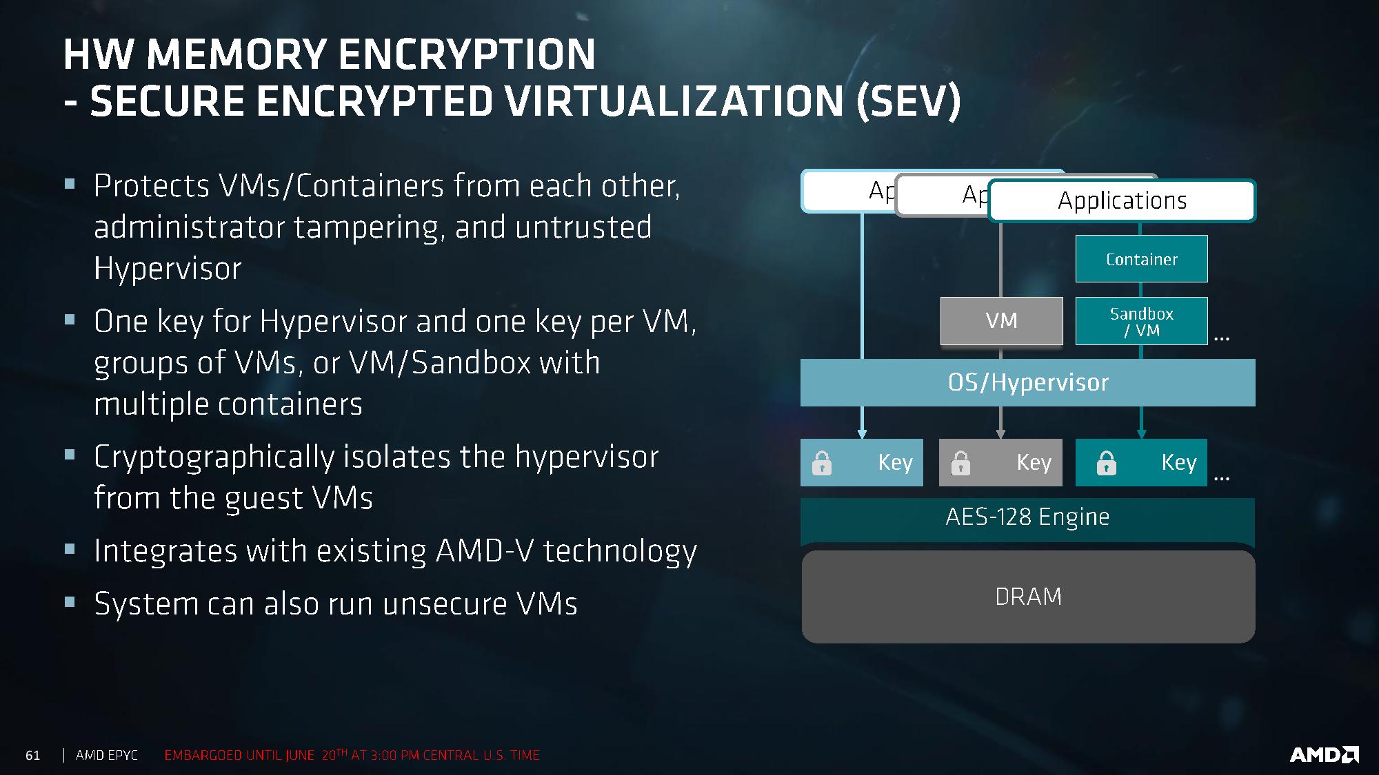
With recent fears about security, and given that these processors are aiming to go to the Enterprise space, AMD had to dedicate some time to explaining how secure the new platform is. AMD has had its Secure Processor in several CPUs at this point: a 32-bit ARM Cortex-A5 acting as a microcontroller that runs a secure OS/kernel with secure off-chip storage for firmware and data – this helps provide cryptographic functionality for secure key generation and key management. This starts with hardware validated boot (TPM), but includes Secure Memory Encryption and Secure Encrypted Virtualization.
Encryption starts at the DRAM level, with an AES-128 engine directly attached to the MMU. This is designed to protect against physical memory attacks, with each VM and Hypervisor able to generate a separate key for their environment. The OS or Hypervisor can choose which pages to encrypt via page tables, and the DMA engines can provide support for external devices such as network storage and graphics cards to access encrypted pages.
Because each VM or container can obtain its own encryption key, this isolates them from each other, protecting against cross-contamination. It also allows unencrypted VMs to run alongside encrypted ones, removing the all-or-nothing scenario. The keys are transparent to the VMs themselves, managed by the protected hypervisor. It all integrates with existing AMD-V technology.
Alongside this are direct RAS features in the core, with the L1 data cache using SEC-DED ECC and L2/L3 caches using DEC-TED ECC. The DRAM support involves x4 DRAM device failure correction with addr/cmd parity and write CRC with replay. Data poisoning is handled with reporting and a machine check recovery mode. The Infinity Fabric between dies and between sockets is also link-packet CRC backed with retry.
One element that was not discussed is live VM migration across encrypted environments. We fully suspect that an AMD-to-AMD live migration be feasible, although an AMD-to-Intel or Intel-to-AMD will have issues, given that each microarchitecture has unique implementations of certain commands.


131 Comments
View All Comments
SodaAnt - Tuesday, June 20, 2017 - link
pJ per bit is a very interesting measurement to use, is this the normal way to measure interconnect power consumption?Ian Cutress - Tuesday, June 20, 2017 - link
Yes :)MrSpadge - Tuesday, June 20, 2017 - link
Yes, unless you're looking at experimental optical interconnects which can reach the fJ/bit range :)ajc9988 - Tuesday, June 20, 2017 - link
https://www.pcper.com/reviews/Processors/Ryzen-5-R...The latency at 2666MHz should be around 120ns, not 140ns, which they got from 2133MHz memory. At 2400MHz, they found 129.62ns.
Gothmoth - Tuesday, June 20, 2017 - link
and you think you can translate that 1:1?to a cpu that has way more security features etc.
cheshirster - Sunday, June 25, 2017 - link
Yes, IF runs at memory speed.All the bandwith and latency numbers are scaling with memory.
ikeke1 - Tuesday, June 20, 2017 - link
https://www.servethehome.com/amd-epyc-7601-dual-so...Crazy numbers.
davegraham - Tuesday, June 20, 2017 - link
it's B2 stepping silicon running ~200-400MHz under the final clocks, fyi.Luckz - Tuesday, June 20, 2017 - link
So with Epyc they made the CCXes NUMA nodes in Windows - https://www.servethehome.com/wp-content/uploads/20...davegraham - Tuesday, June 20, 2017 - link
you can flatten the NUMA domains via BIOS hooks to just 1 or 2 per processor but there is a relative hit to latency. this is the "downside" to a MCM-based processor vs. ring/monolithic mesh. however, the upside IS agility based on chip packaging and time to market so....there's always a cost/benefit ratio to consider.