AMD's Future in Servers: New 7000-Series CPUs Launched and EPYC Analysis
by Ian Cutress on June 20, 2017 4:00 PM EST- Posted in
- CPUs
- AMD
- Enterprise CPUs
- EPYC
- Whitehaven
- 1P
- 2P
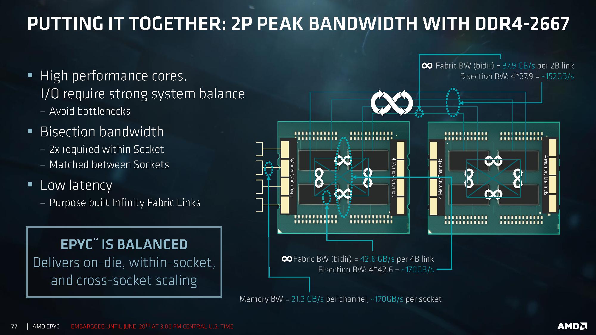
NUMA NUMA IEI: Infinity Fabric Bandwidths
The news about AMD using four Zeppelin dies from Ryzen to form EPYC is not new news, having been shown several times before. However, given the design of the silicon and how the cores communicate, there has been a few worries about how the intra-package communications will be affected by not being a single monolithic die. Beyond that, socket-to-socket communications can also be an issue without sufficient latency and bandwidth.
In a single monolithic die, the latency to access other cores is usually a predictable average, with a regular latency and bandwidth out to the memory channels. Because EPYC has two memory channels per die, if a core needs to access DRAM associated with another die, it adds additional hops and latency to the access, slowing down potential instruction throughput. In the land of dual socket systems, this is known as NUMA: Non-Unified Memory Architecture. The way around a NUMA environment is data locality – keeping the data that a core needs as close as feasibly possible. Solving NUMA is a difficult task, and attempted both at the silicon and software level. Most high-end professional software packages designed for dual-socket systems are NUMA aware, and are designed to compensate for this. The majority of non-high-end software though, is not.
Intra-Socket
With the quad-die design, a single EPYC processor might essentially have four zones for NUMA to occur, based on communication paths. AMD went to specifically address this issue in their design briefings.
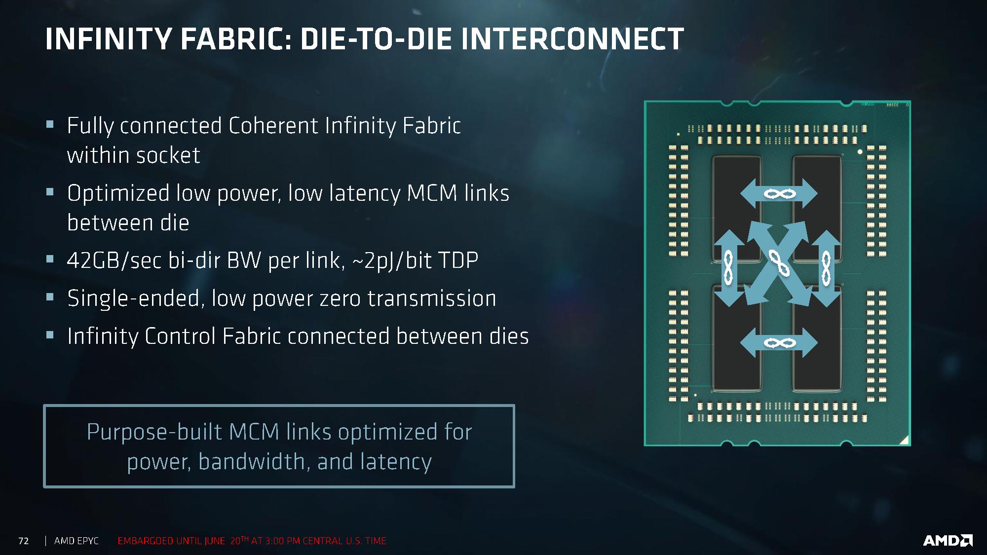
Within a single processor, each of the three dies is directly linked to each other through the Infinity Fabric, so only one hop is ever needed when data goes off-die. The connectivity here is set at a bidirectional 42.6 GB/sec per link, at around an average energy of ~2 pJ per bit (or 0.672W per link, 0.336W per die per link, totaling 4.032W for the chip). It is worth noting that Intel’s eDRAM for Broadwell was set as a 50 GB/s bidirectional link, so in essence moving off die in EPYC has a slightly slower bandwidth than Crystalwell. With a total of six links within the silicon, that provides a total of 2 terabits per second of data movement, although AMD didn’t state what the bottlenecks or latency values were.
Inter-Socket
Socket-to-socket communication is designed at the die level, rather than going through a singular interface. One die in each processor is linked to the same die in the other processor, meaning that for the worst-case scenario data has to make two hops to reach a core or memory controller on the other side of the system. Each link has a bidirectional 37.9 GB/s bandwidth, which is only slightly less than the intra-socket communication bandwidth, although we would expect socket-to-socket to have a slightly higher latency based on distance. AMD has not shared latency numbers at this time.
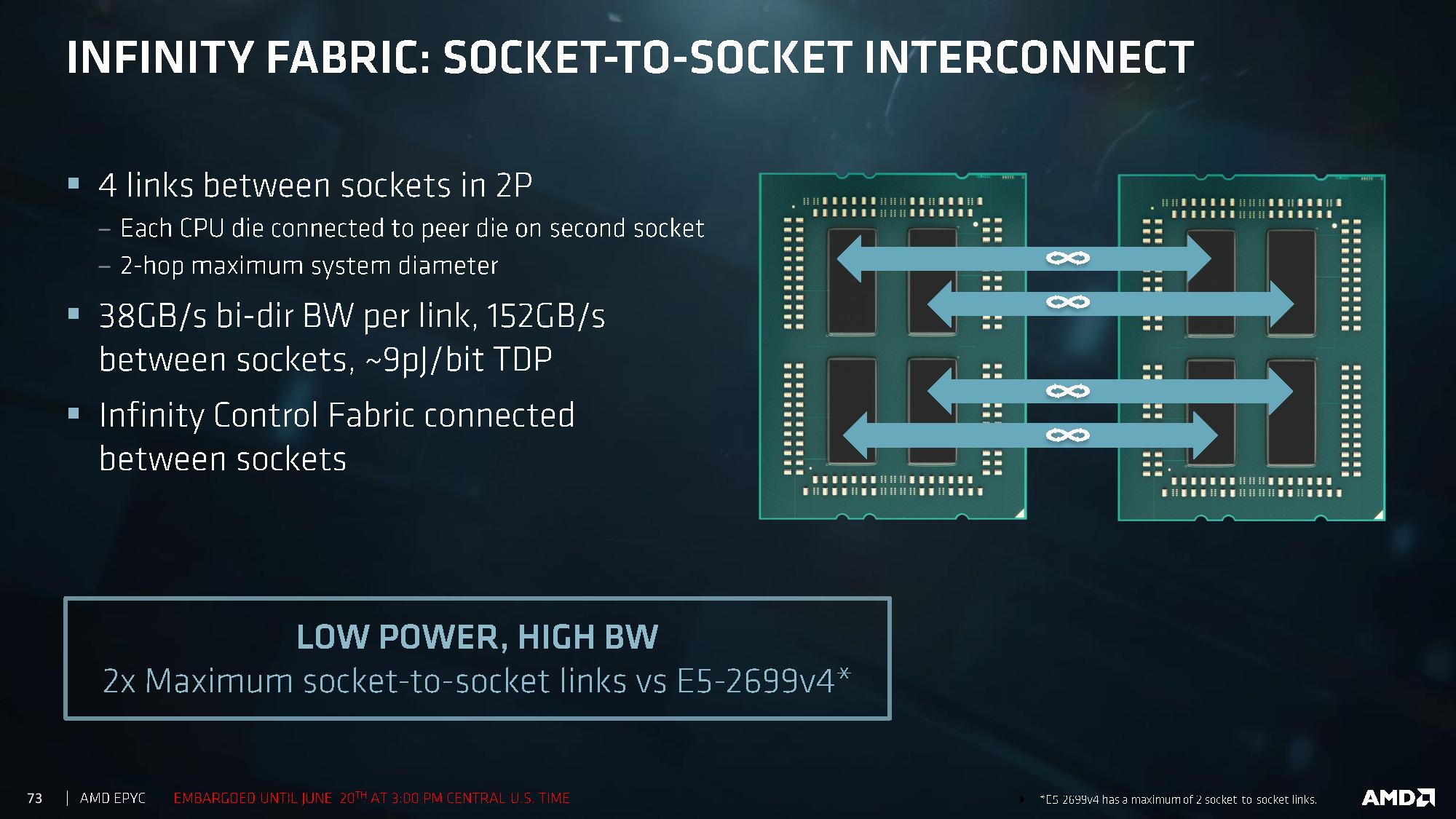
At 37.9 GB/s per link, this totals 152 GB/s between sockets, which AMD states runs at an average of 9 pJ per bit. So at full speed, this link will consume 10.94W between the two sockets, or 5.48W per processor and 1.368W per silicon die.
Totaling the 1.368W per die for socket-to-socket plus 3*0.336W per die for intra-socket communications, the Infinity Fabric can consume 2.376W per silicon die on average when going at full speed.
Infinity Fabric Latency
AMD has not provided Infinity Fabric numbers for latency. We are waiting on information, but this is likely going to be a critical answer for some software packages. Based on testing done by PC Perspective, we already know some latency numbers within a single Zeppelin die from the Ryzen platform. This allows us to fill in the following table showing how long it takes to ping another core:
| EPYC (Naples) Thread Ping Connections | ||
| Latency | Bandwidth | |
| Within A Core | 26 ns | - |
| Core-to-Core, Same CCX | 42 ns | - |
| Core-to-Core, Different CCX, Same Die | 142 ns | - |
| Die-to-Die, Same Package | ? | 42.6 GB/s |
| Die-to-Die, Different Socket, One Hop | ? | 37.9 GB/s |
| Die-to-Die, Different Socket, Two Hops | ? | 37.9 GB/s |
| Core to DRAM, Same Die | ? | 42.6 GB/s |
| Core to DRAM, Different Die | ? | 42.6 GB/s |
| Core to DRAM, Different Socket, One Hop | ? | 37.9 GB/s |
| Core to DRAM, Different Socket, Two Hops | ? | 37.9 GB/s |
PCIe Bandwidth
Each Zeppelin die can create two PCIe 3.0 x16 links, which means a full EPYC processor is capable of eight x16 links totaling the 128 PCIe lanes presented earlier. AMD has designed these links such that they can support both PCIe at 8 GT/s and Infinity Fabric at 10.6 GT/s, although in PCIe mode this means 32GB/s of bidirectional bandwidth per link, suitable for 256GB/s per socket. One of AMD’s proposed benefits here is link bifurcation support:
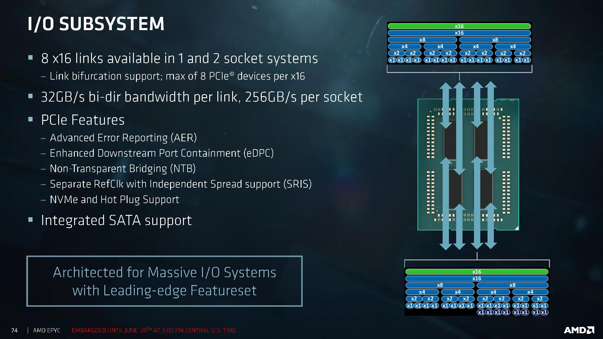
Each x16 link can support Infinity Fabric (green), PCIe (blue) and SATA (dark blue). PCIe can be bifurcated all the way down to sets of x1, although there will be a limit of 8 PCIe devices per x16 link, but this becomes a mix and match game: x8 + x4 + x2 + x1 + x1 + x1 + x1 becomes entirely valid for a single x16 link, and each CPU has eight of these such links. For the SATA connectivity, each x16 link can support 8 SATA drives as a result. If you really want 64 devices per processor, welcome to your platform without buying PCIe switches. AMD states that as an NVMe implementation, supporting 32 NVMe devices is going to be no sweat for an EPYC system.
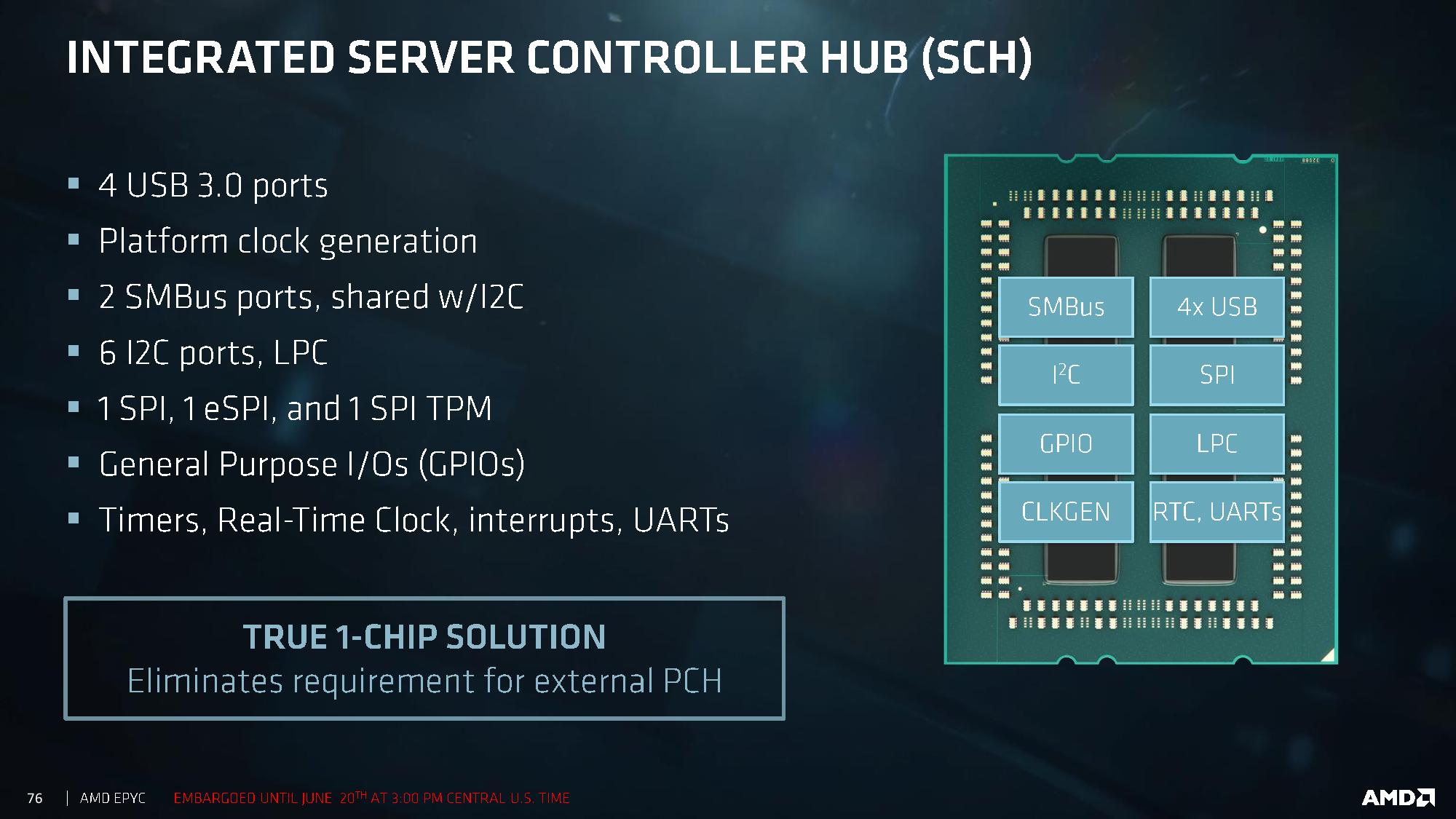
This also relates to the Sever Controller Hub, which acts as part of the design offering four USB 3.0 ports, SMBus, I2C, SPI, eSPI, TPM, GPIOs, timers and UARTs.
Combining The Bandwidth
Altogether, AMD is stating that they are relatively unconcerned about NUMA related issues, with bandwidth between dies and between sockets being relatively similar. It is worth noting that the 42.6 GB/s die-to-die bandwidth is identical to the dual-channel memory bandwidth quoted per die:
Time will tell if these become bottlenecks. Latency numbers please, I’d love to fill in that table above.


131 Comments
View All Comments
deltaFx2 - Wednesday, June 21, 2017 - link
That's because intel cheats on SPEC in icc by doing transformations that are specifically targetted at making SPEC faster and nothing else. Libquantum is a particularly egregious example where you nearly double the performance by doing tricks that help nothing else. But this is generally true across the suite. It's not unlike VW's emission defeat devices: do something special when you're being tested.As for Tom's hardware, they're not authorities on anything server. What they know something about is gaming benchmarking, and that's pretty much it. I don't expect he'd know a thing about it, and whether 20% is correct vs 40%. It's a feeble attempt at sounding clever. The people buying this stuff know what they're doing, and aren't going to be influenced by some online reviewer.
Ryan Smith - Tuesday, June 20, 2017 - link
I've posted galleries of the full slide decks. The slide you're interested in is: http://images.anandtech.com/galleries/5699/epyc_te..."Scores for these E5 processors extrapolated from test results published at www.spec.org, applying a conversion multiplier to each published score"
patrickjp93 - Wednesday, June 21, 2017 - link
No, it vastly underestimates and undermines Intel's real-world performance.lefty2 - Tuesday, June 20, 2017 - link
I think you missed the point of the eight-core processor. That's for GPU compute servers, where you want the cheapest processor possible with the most PCIe lanes. It's probably going to be the one that sells the most, because Intel has nothing comparable.Luckz - Tuesday, June 20, 2017 - link
Is this useful for the mining craze?LurkingSince97 - Tuesday, June 20, 2017 - link
probably not. Miners want the most GPU (hashes) per Watt (combined with total price). If they can do that with 5 smaller, cheaper machines vs 1 larger one, they will. Mining does not need coordination across multiple GPUs.The enterprisey compute stuff -- machine learning being a huge one -- often _does_ need to coordinate across GPUs in one big data set and will run in datacenters where consolidation into performance/$ and performance/Watt will often like servers with few CPU and many GPU, with a ton of I/O and connectivity to other servers.
Mining doesn't care about I/O, just total # of ports. People even use tools to split up a x16 bus of a normal consumer motherboard into may smaller PCIe ports each with a GPU on it. The GPU will compute hashes just as well with a x2 port as a x16 one.
KAlmquist - Wednesday, June 21, 2017 - link
EPYC has 128 PCI-e lanes on both 1 socket and 2 socket systems, so if AMD had intended the EPYC 7251 to be used for GPU compute servers, they would have made it part of the single socket lineup. That doesn't mean that the chip won't be used in GPU compute servers; it just means that GPU compute servers are not the market that AMD intended to target with the chip.Zizy - Thursday, June 22, 2017 - link
All these 2P Epyc CPUs should be just fine in 1P as well. Obviously nobody will buy most of them to run in 1P, as 1P are cheaper. It is just 1P that is limited - it can be *only* used in 1P.And given 500-ish price of the chip, I can see why AMD didn't bother to give additional 400 chip for 1P - it wouldn't change anything. And limiting this chip to just 1P would be pointless, as the other segments such as "need tons of memory" would be hurting for no good reason.
armtec - Tuesday, June 20, 2017 - link
NUMA NUMA IEI... I hadn't previously made this connection but now I will every time I need to think about server configs...Barilla - Tuesday, June 20, 2017 - link
I read that header and now that stupid song will be stuck in my head for days...