The Intel Skylake-X Review: Core i9 7900X, i7 7820X and i7 7800X Tested
by Ian Cutress on June 19, 2017 9:01 AM ESTThe New Core-to-Core Communication Paradigm
Within the last week, Intel released a surprising announcement regarding the capability of its upcoming Skylake-SP processors ahead of any official announcement and release, and the relevance of it extends through to the Skylake-X chips as well. With a multi-core design, how cores communicate can be vital, when sharing data between them or by accessing each other’s cache via snooping or having to go out to main memory.
In previous generations, Intel has championed its ring bus strategy. Pretty much every commercial multi-core chip Intel has released uses some form of ring bus, and it boils down to a single communication ring on which all the cores are connected. If data needs to a certain core, it travels on the ring until it reaches the core it needs. The idea is relatively simple, and has worked quite well. It does mean that there is a range of core-to-core latencies however, depending on how far away the core is.
Imagine connecting to a network of computers, but you could only connect to the two computers either side of you. If you needed to speak to a computer that was 5 nodes away, the data would have to travel through each of the nodes to get there. Welcome to the ring bus. The speed of this ring bus was typically denoted by the ‘uncore’ frequency.
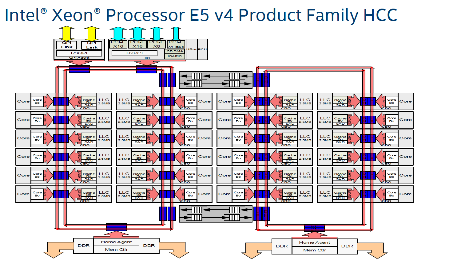
With Intel’s three-die program on its enterprise chips, each one used different variants of the ring bus topology. On Broadwell-E, the 10-core LCC design used a single ring bus for all 8 cores and the DRAM controller/PCIe root complex, whereas the HCC and XCC designs both had dual ring buses that used router communication methods to talk between each other. Now obviously talking to a core on the other ring bus added latency, and was sometimes considered a ‘non-uniform memory access’ (NUMA) environment on chip, with extra latency if you needed data from memory on the other ring bus. (Typically NUMA is applied to dual socket platforms, where the DRAM on the other chip has a large delay.) Intel emphasized that the Broadwell-E design was memory location aware, and tried to keep relevant data local to the core it was needed on.
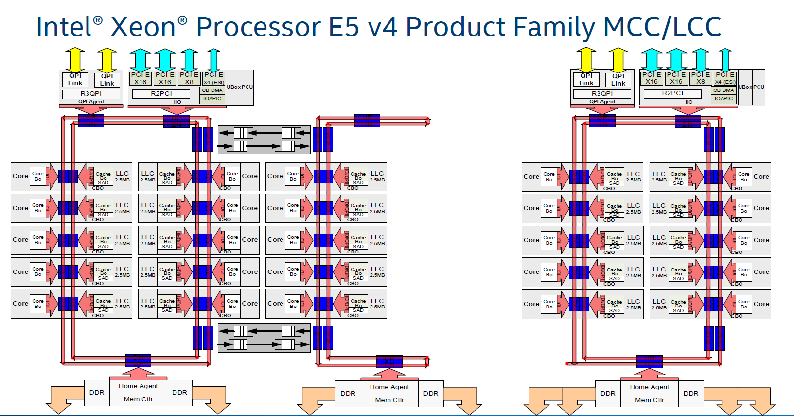
With the larger XCC CPUs for Broadwell-E, the ring buses become quite cumbersome: you end up with one ring bus servicing 12 cores, and another ring bus servicing 12 cores (due to the layout with other elements of the chip).
As more and more cores get added, what is the solution? More ring buses? How about a 2D array of ring buses? Or even a mesh or a network?

The announcement that Intel made in the past week was that Skylake-SP processors will use a mesh topology, whereby each CPU in the design will be connected to the ones above, below, and to the side. Earlier in the week I mentioned on Twitter that a mesh in this context, or as drawn above, is just an array of ring buses in a 2D arrangement, although new information has come to light.
There are several things to talk about the mesh here, so in no particular order:
Mesh Me Up
Intel already sells chips with mesh connectivity: the latest Xeon Phi Knights Landing many-core processors. These massive (~646mm2) chips have 72 cores arranged as 36 pairs, six memory channels and 16GB of MCDRAM, and using a ring bus (or a succession of ring buses) is probably not feasible.
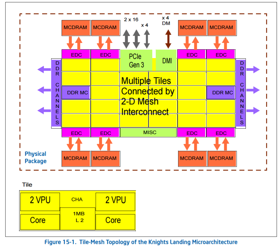
For KNL, Intel calls the mesh the ‘untile’. Taken from the KNL optimization guide:
‘At each mesh stop, there is a connection to the tile and a tag directory that identifies which L2 cache (if any) holds a particular cache line. [In Knights Landing] there is no shared L3 cache within a physical package, [so] memory accesses that miss in the tile must go over the mesh to the tag directory to identify any cached copies in another tile. Cache coherence uses the MESIF protocol. If the cache line is not cached in another tile, then a request goes to memory.’
Knights Landing can run in a variety of mesh modes, due to the lack of an L3 but the presence of an intermediary MCDRAM layer, certain modes to do with the memory hierarchy help with different codes. It is not known if Skylake-SP will have the same feature set.
When distributing cores along a mesh, another way to think about it is as a big routing environment. There are two ways – each core could talk to a central processing router which then sends information as it is needed, or each core acts as a networking point itself, forwarding packets in the direction it is needed. The first method, commonly known as a crossbar method, is easier to implement but can be bottlenecked very easily, not to mention power hungry if the whole crossbar needs to be enabled all the time. The second method, where every core is a router node, looks like what we have already in the image Intel provided.
The announcement Intel made was done officially by Dr Akhilesh Kumar, one of Skylake-SP’s CPU architects. He has been at Intel for a number of years, and digging back through releases with his name on popped up a very interesting paper regarding how to implement a router-like mesh in a multi-core environment, published in March 2014 which is about the right time when Skylake-SPs mesh was being developed. We haven’t had confirmation from Intel that this is how Skylake-SP’s mesh is actually like, though it is worth covering what is in the paper.
For anyone interested, the paper is called MoDe-X: Microarchitecture of a Layout-Aware Modular Decoupled Crossbar for On-Chip Interconnects, IEEE Transactions on Computers, Vol. 63, No. 3, March 2014 P622.
MoDe-X: Is This Skylake-SP’s Mesh?
As mentioned above, the easiest way for a mesh/router is through a crossbar. When the design instead uses each core as a node in the mesh, the result is essentially a ‘mini’ decoupled crossbar in each core acting as the director for data coming in and out of the core. With each core in control of its own actions, the design becomes modular. Put these elements together, and you have a MOdular DEcoupled Crossbar, or MoDe-X.
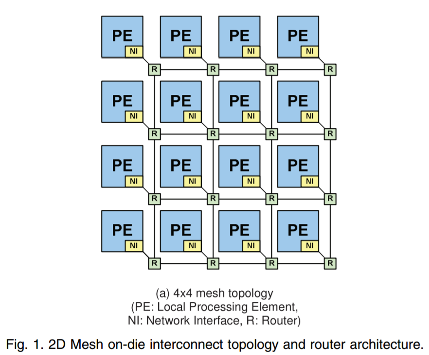
Each core has an integrated network interface and a router, with each router connected to the four routers around it (or 2 routers for corners and 3 routers for edges). A data packet can come in one of five directions – north, south, east, west, or from the core the router is attached to. The data packet then needs to be sent to one of five directions again: north, south, east, west, or to the core the router is attached to. If each core is essentially a node on a 2D map with an x-ordinate and a y-ordinate, if a packet needs to go to (0,0), the router can send it on its way as it knows which nodes are nearest to it. There are algorithms designed to reduce congestion, such as only moving in the x-direction until you are correct then start moving in the y-direction, but a basic system will have buffers and queues and will know how busy the local network congestion is.
The default way to design the router is to take the date from every input, decided where to send it, then send it. The MoDe-X design does it a little differently, and essentially splits the directions up into three groups: one group is north/south, one group is east/west, and the local core is the third group. The following diagram is a bit complex, but we’ll go through it:
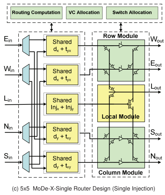
On the left are the five inputs: E, W, L (local), N, S.
On the right are the five outputs, W, E, L, S, N
The first column of ‘shared’ boxes determines where the data wants to go: does it need to traverse a row, a column, or stay local. From each input, there are only two arrows going to either the top pair or the bottom pair of ‘shared’ boxes. Depending on contention and allocation, the data is then sent to the second column whereby if the data needed to change columns, it could either go to Sout or Nout and if it needed to change rows into Wout or Eout. In both circumstances the data could go to the local node.
In the research paper, there is a six-input design which modifies the local input in order to make the wiring in the second half of the design easier (and it lowers power), but the image above is a fair representation of the idea. There are other additions in the paper as well, with layout aware arrangements (how exactly you put it together in silicon) as well as feeder wires such that if data needs to continue in the same direction it can do so with less effort.
The paper is very dense (it took me a while to get to grips with it), but worth a read if you are interested. I found it easier to consider it more like a router, than an on-chip mesh. As mentioned, this is a 2014 paper, and shows simulation data on an 8x8 grid of cores, where this design is both lower power and smaller area than a generic mesh design or competing designs. There were some areas where the generic design had marginally better latency, but the power conservation numbers (due to the wiring reduction and an aggressive power gating scheme to disable certain parts for up to 99% less power use) makes it a more attractive option (especially in multi-core CPUs). Intel was doing simulation work in early 2014 (which means 2013), and the paper mentions that they were in the process of putting these ideas into silicon. It wouldn’t be too far-fetched to consider that this is what we are seeing today.


264 Comments
View All Comments
Tephereth - Tuesday, June 20, 2017 - link
"For each of the GPUs in our testing, these games (at each resolution/setting combination) are run four times each, with outliers discarded. Average frame rates, 99th percentiles and 'Time Under x FPS' data is sorted, and the raw data is archived."So... where the hell are the games benchmarks in this review?
beck2050 - Tuesday, June 20, 2017 - link
The possibility of the 18 core beast in the upcoming Mac Pro is really exciting for music pros.That is a tremendous and long overdue leap for power users.
drajitshnew - Tuesday, June 20, 2017 - link
"... and only three PCIe 3.0 x4 drives can use the in-built PCIe RAID"I would like to know which raid level you would use. I can't see 3 m2 drives in raid 1, and raid 5 would require access to the cpu for parity calculations. Then raid 0 it is. Now, which drives will you use for raid 0, which do not saturate the DMI link for sequential reads? And if your workload does not have predominantly sequential reads, then why are you putting the drives in raid.
PeterCordes - Tuesday, June 20, 2017 - link
Standard motherboard RAID controllers are software raid anyway, where the OS drivers queue up writes to each drive separately, instead of sending the data once over the PCIe bus to a hardware RAID controller which queues writes to two drives.What makes it a "raid controller" is that you can boot from it, thanks to BIOS support. Otherwise it's not much different from Linux or Windows pure-software RAID.
If the drivers choose to implement RAID5, that can give you redundancy on 3 drives with the capacity of 2.
However, RAID5 on 3 disks is not the most efficient way. A RAID implementation can get the same redundancy by just storing two copies of every block, instead of generating parity. That avoids a ton of RAID5 performance problems, and saves CPU time. Linux md software RAID implements this as RAID10. e.g. RAID10f2 stores 2 copies of every block, striped across as many disks as you have. It works very well with 3 disks. See for example https://serverfault.com/questions/139022/explain-m...
IDK if Intel's mobo RAID controllers support anything like that or not. I don't use the BIOS to configure my RAID; I just put a boot partition on each disk separately and manage everything from within Linux. IDK if other OSes have soft-raid that supports anything similar either.
> And if your workload does not have predominantly sequential reads, then why are you putting the drives in raid.
That's a silly question. RAID0, RAID1, and RAID5 over 3 disks should all have 3x the random read throughput of a single disk, at least for high queue depths, since each disk will only see about 1/3rd of the reads. RAID0 similarly has 3x random write throughput.
RAID10n2 of 3 disks can have better random write throughput than a single disk, but RAID5 is much worse. RAID1 of course mirrors all the writes to all the disks, so it's a wash for writes. (But can still gain for mixed read and write workloads, since the reads can be distributed among the disks).
Lieutenant Tofu - Tuesday, June 20, 2017 - link
I wonder why 1600X outperforms 1800X here on WebXPRT. It's not a huge difference, but I don't see why it's happening. 6-core vs. 8-core, 3.6 GHz base, 4.0 GHz turbo. This presumably runs in just one thread, so performance should be nearly identical. The only reason I can think of is less contention across the IF on the 1600X due to less enabled cores, but don't see that having a major effect on a single-threaded test like this one.Maybe 1600X can XFR to a little higher than the 1800X.
Eyered - Tuesday, June 20, 2017 - link
Did they have any issues with heat at all?mat9v - Tuesday, June 20, 2017 - link
If that were so everyone would be using HEDT instead of 4c/8t CPUsmat9v - Tuesday, June 20, 2017 - link
Then why again why aren't every workstation consist of dual cpu xeons? If the expense is so insignificant compared to how much faster machine will earn...mat9v - Tuesday, June 20, 2017 - link
I'm just wondering how did 7900X menage to stay within 140W bracket during Prome95 tests when in other reviews it easily reached 250W or more. Is it some internal throttling mechanism that keeps CPU constantly dynamically underclocked to stay within power envelope? How does such compare to forced 4Ghz CPU clock?mat9v - Tuesday, June 20, 2017 - link
And yet in conclusion you say to play it safe and get 7900X ?How does that work together?