Sizing Up Servers: Intel's Skylake-SP Xeon versus AMD's EPYC 7000 - The Server CPU Battle of the Decade?
by Johan De Gelas & Ian Cutress on July 11, 2017 12:15 PM EST- Posted in
- CPUs
- AMD
- Intel
- Xeon
- Enterprise
- Skylake
- Zen
- Naples
- Skylake-SP
- EPYC
Intel’s Skylake-SP Processors: Platinum, Gold, Silver, Bronze
In a break from the traditional naming scheme that Intel has used for several generations, we saw the move to Platinum, Gold, Silver and Bronze SKUs for Skylake-SP. We’re told there is no real conversion between the two, and to some extent Intel is correct: it’s almost impossible to correlate what the conversion from the old chip naming is to the new chip naming is, but also Intel has decided to awkwardly complicate what the numbers in the middle mean, with no real direct pattern to follow on some of the digits. This is the diagram provided:
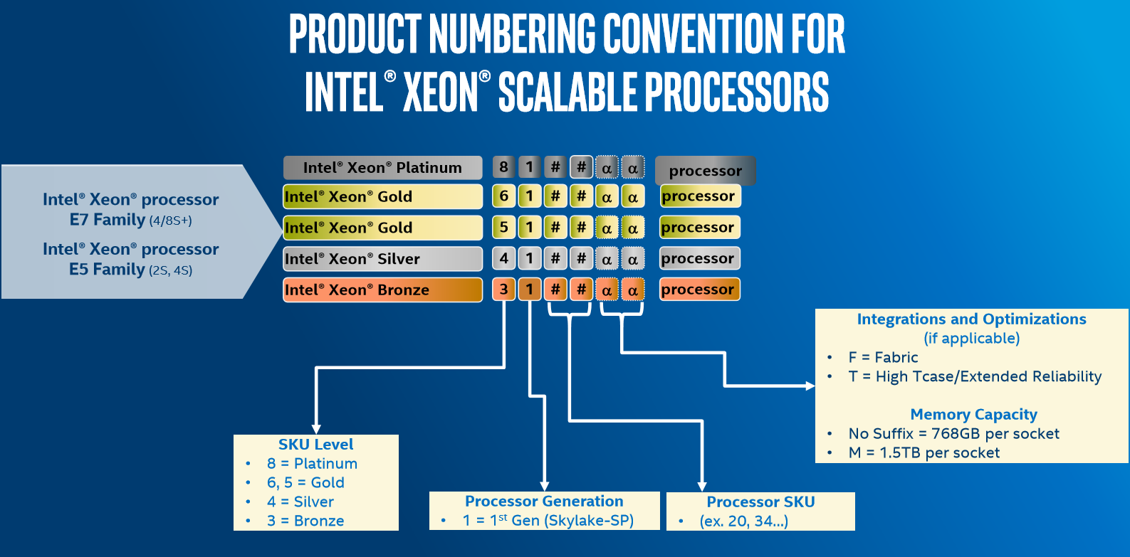
Aside from the name (Platinum, Gold, Silver, Bronze), the four digits indicate SKU level, Generation, and then a pair of digits for general performance level. After this there are a series of potential suffixes:
- M = Supports 1.5 TB DRAM per socket, up from 768GB as standard
- T = High T-Case, Extended Life
- F = Integrated OmniPath Fabric
This leads to the following lists for the processors. We have sorted these into numerical order, which may be different to Intel’s pricing or specification lists. First up is the Platinum parts, geared for up to 8-Socket use.
Xeon Platinum
So what is the "Platinum" all about? We were told at the briefing:
"One of the reasons for this is that sometimes a customer could take advantage of an 8-socket variant processor (due to high cache per core, for example), but would never consider it because the customer only needed a two-socket configuration. One of the reasons given for the naming is to alleviate this issue."

There is no longer an E7, but if you look at the prices ($3000-$13000) and features, the Xeon Platinum is clearly the successor to the E7. There is support for up to 8 sockets, and most of the Platinum SKUs have 24 to 28 cores, and is clearly using the XCC silicon.
| Intel Xeon Skylake-SP Platinum Series | ||||||||||
| Segment | Cores | Base (GHz) |
Turbo (GHz) |
L3 (MB) |
L3/core (MB) |
TDP (W) |
Price (USD) |
|||
| 8180 | Per-Core | 28 | 2.5 | 3.8 | 38.50 | 1.375 | 205 | $10009 | ||
| 8180 | M | 2xDRAM | 28 | 2.5 | 3.8 | 38.50 | 1.375 | 205 | $13011 | |
| 8176 | Perf/Watt | 28 | 2.1 | 3.8 | 38.50 | 1.375 | 165 | $8719 | ||
| 8176 | M | 2xDRAM | 28 | 2.1 | 3.8 | 38.50 | 1.375 | 165 | $11722 | |
| 8176 | F | OmniPath | 28 | 2.1 | 3.8 | 38.50 | 1.375 | 173 | $8874 | |
| 8170 | Perf/Watt | 26 | 2.1 | 3.7 | 35.75 | 1.375 | 165 | $7405 | ||
| 8170 | M | 2xDRAM | 26 | 2.1 | 3.7 | 35.75 | 1.375 | 165 | $10409 | |
| 8168 | Per-Core | 24 | 2.7 | 3.7 | 33.00 | 1.375 | 205 | $5890 | ||
| 8164 | Perf/Watt | 26 | 2.0 | 3.7 | 35.75 | 1.375 | 150 | $6114 | ||
| 8160 | Perf/Watt | 24 | 2.1 | 3.7 | 33.00 | 1.375 | 150 | $4702 | ||
| 8160 | M | 2xDRAM | 24 | 2.1 | 3.7 | 33.00 | 1.375 | 150 | $7704 | |
| 8160 | T | 10yr Life | 24 | 2.1 | 3.7 | 33.00 | 1.375 | 150 | $4936 | |
| 8160 | F | OmniPath | 24 | 2.1 | 3.7 | 33.00 | 1.375 | 160 | $4856 | |
| 8158 | Per-Core | 12 | 3.0 | 3.7 | 24.75 | 2.063 | 150 | $7007 | ||
| 8156 | Per-Core | 4 | 3.6 | 3.7 | 16.50 | 4.125 | 105 | $7007 | ||
| 8153 | Perf/Watt | 16 | 2.0 | 2.8 | 22.00 | 1.375 | 125 | $3115 | ||
I suppose the first thing to note is the pricing. If you want the extended DRAM version of the 28-core CPU, be prepared to shell out $13k for the tray pricing. That is almost 2x the cost of the highest-end previous generation part, and becomes a sizeable chunk of any build. The standard DRAM support version is ‘only’ $10k. For anyone around the $7-8k per CPU budget, like last generation, you can still get a 28-core processor in the form of the 8176, or 8170 if you can give up a couple of cores.
With the double DRAM supported parts, the 30% premium seems rather high. We were told from Intel that ‘only 0.5% of the market actually uses those quad ranked and LR DRAMs’, although that more answers the fact that the base support is 768GB, not that the 1.5GB parts have an extra premium.
This pricing seems crazy, but it is worth pointing out a couple of things. The companies that buy these parts, namely the big HPC clients, do not pay these prices. They’ll likely pay under half these prices, and probably much less. Nonetheless, this is still a sizeable jump over the last generation – exact pricing for the top tier customers will be in their contracts, but it has been predicted by some analysts that there might be a small outcry, even from Intel’s largest customers.
A few users might be confused about the Platinum 8156, a quad core part at $7007. This is a high cache/core part, offering 4.125 MB of L3 per core, up from 1.375MB per core for the standard parts. Intel has offered these parts for a few generations now, for customers that find their code to be L3 sensitive or have licensing agreements base on per-core/per-socket as well. What customers will have to note is that Skylake-SP has a different L3 cache compared to previous generations, by being a non-inclusive cache (and essentially a victim cache) means it will be used very differently. With a larger L2 cache as well, the L3 might become less important, or the fact it becomes a victim cache might make it useful/useless on the code. For customers after these sorts of cores, it is worth profiling the code on the CPU first, just to make sure.
Xeon Gold
Despite some of the nuance, the Platinum processor list is easy to follow, especially by comparison to the Gold list. The Gold processors are technically split into two groups, the Gold 6100 series, and Gold 5100 series: split in their DRAM and AVX-512 support, as well as the number of UPI links.
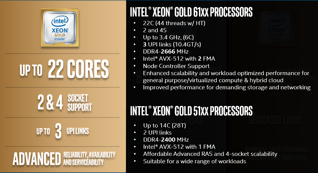
The Gold 6100-series will have 2 FMA units per core rather than one, showing that the Port-5 FMA is enabled and can feed the AVX-512 unit better for up to 2x performance. (This is similar to what we saw with the consumer Skylake-X parts, where >10-core parts have both FMAs enabled.) The 6100-series also has DDR4-2666 support, whereas the 5100-series is limited to DDR4-2400 as standard.
There’s also a matter of UPI links to other processors. This matters when these processors are in a quad-socket system: with only 2 UPI links for the 5100-series, that means the processors are in a ring arrangement, rather than a hatch-arrangement, and to access data on the opposite side of the ring requires two hops, rather than the one hop on the hatch. This is perhaps a niche issue, but one worth taking note of.
| Intel Xeon Skylake-SP Gold Series | ||||||||||
| Segment | Cores | Base (GHz) |
Turbo (GHz) |
L3 (MB) |
L3/core (MB) |
TDP (W) |
Price (USD) |
|||
| 6154 | Per-Core | 18 | 3.0 | 3.7 | 24.75 | 1.375 | 200 | $3543 | ||
| 6152 | Perf/Watt | 22 | 2.1 | 3.7 | 30.25 | 1.375 | 140 | $3655 | ||
| 6150 | Per-Core | 18 | 2.7 | 3.7 | 24.75 | 1.375 | 165 | $3358 | ||
| 6148 | Per-Core | 20 | 2.4 | 3.7 | 27.50 | 1.375 | 150 | $3072 | ||
| 6148 | F | OmniPath | 20 | 2.4 | 3.7 | 27.50 | 1.375 | 160 | $3227 | |
| 6146 | Per-Core | 12 | 3.2 | 4.2 | 24.75 | 2.063 | 165 | $3286 | ||
| 6144 | Per-Core | 8 | 3.5 | 4.2 | 24.75 | 3.094 | 150 | $2925 | ||
| 6142 | Per-Core | 16 | 2.6 | 3.7 | 22.00 | 1.375 | 150 | $2946 | ||
| 6142 | M | 2x DRAM | 16 | 2.6 | 3.7 | 22.00 | 1.375 | 150 | $5949 | |
| 6142 | F | OmniPath | 16 | 2.6 | 3.7 | 22.00 | 1.375 | 160 | $3101 | |
| 6140 | Perf/Watt | 18 | 2.3 | 3.7 | 24.75 | 1.375 | 140 | $2445 | ||
| 6140 | M | 2x DRAM | 18 | 2.3 | 3.7 | 24.75 | 1.375 | 140 | $5448 | |
| 6138 | Perf/Watt | 20 | 2.0 | 3.7 | 27.50 | 1.375 | 125 | $2612 | ||
| 6138 | T | 10yr Life | 20 | 2.0 | 3.7 | 27.50 | 1.375 | 125 | $2742 | |
| 6138 | F | OmniPath | 20 | 2.0 | 3.7 | 27.50 | 1.375 | 135 | $2767 | |
| 6136 | Per-Core | 12 | 3.0 | 3.7 | 24.75 | 2.063 | 150 | $2460 | ||
| 6134 | Per-Core | 8 | 3.2 | 3.7 | 24.75 | 3.094 | 130 | $2214 | ||
| 6134 | M | 2x DRAM | 8 | 3.2 | 3.7 | 24.75 | 3.094 | 130 | $5217 | |
| 6132 | Per-Core | 14 | 2.6 | 3.7 | 19.25 | 1.375 | 140 | $2111 | ||
| 6130 | Perf/Watt | 16 | 2.1 | 3.7 | 22.00 | 1.375 | 125 | $1894 | ||
| 6130 | T | 10yr Life | 16 | 2.1 | 3.7 | 22.00 | 1.375 | 125 | $1988 | |
| 6130 | F | OmniPath | 16 | 2.1 | 3.7 | 22.00 | 1.375 | 135 | $2049 | |
| 6128 | Per-Core | 6 | 3.4 | 3.7 | 19.25 | 3.208 | 115 | $1691 | ||
| 6126 | Per-Core | 12 | 2.6 | 3.7 | 19.25 | 1.604 | 125 | $1776 | ||
| 6126 | T | 10yr Life | 12 | 2.6 | 3.7 | 19.25 | 1.604 | 125 | $1865 | |
| 6126 | F | OmniPath | 12 | 2.6 | 3.7 | 19.25 | 1.604 | 135 | $1931 | |
| 5122 | Per-Core | 4 | 3.6 | 3.7 | 16.50 | 4.125 | 105 | $1221 | ||
| 5120 | Perf/Watt | 14 | 2.2 | 3.2 | 19.25 | 1.375 | 105 | $1555 | ||
| 5120 | T | 10yr Life | 14 | 2.2 | 3.2 | 19.25 | 1.375 | 105 | $1727 | |
| 5119 | T | 10yr Life | 14 | 1.9 | - | 19.25 | 1.375 | 85 | $1555 | |
| 5118 | Perf/Watt | 12 | 2.3 | 3.2 | 16.50 | 1.375 | 105 | $1273 | ||
| 5115 | Perf/Watt | 10 | 2.4 | 3.2 | 13.75 | 1.375 | 85 | $1221 | ||
Why all those differences between the two grades of Gold did not result in a separate "grade" for the 51xx is beyond me. For example, for the HPC people, the 51xx gets you slower DRAM and half the FP peak performance. The only logical way to describe the Gold grade is "the 4 socket version with wildly varying features".
Xeon Silver and Xeon Bronze
After 16 CPUs for Platinum and 32 CPUs in Gold, the Silver and Bronze parts only have 10 in total. These parts support two sockets at most, and only up to 12 cores, showing that Intel’s market segmentation strategy has changed significantly here. In the last generation, a customer could get a dual-socket high-core-count part like the E5-2699A v4 without the need to look at 8-socket parts, but now Intel has that limited such that you have to look at Gold or Platinum processors to play in this space.
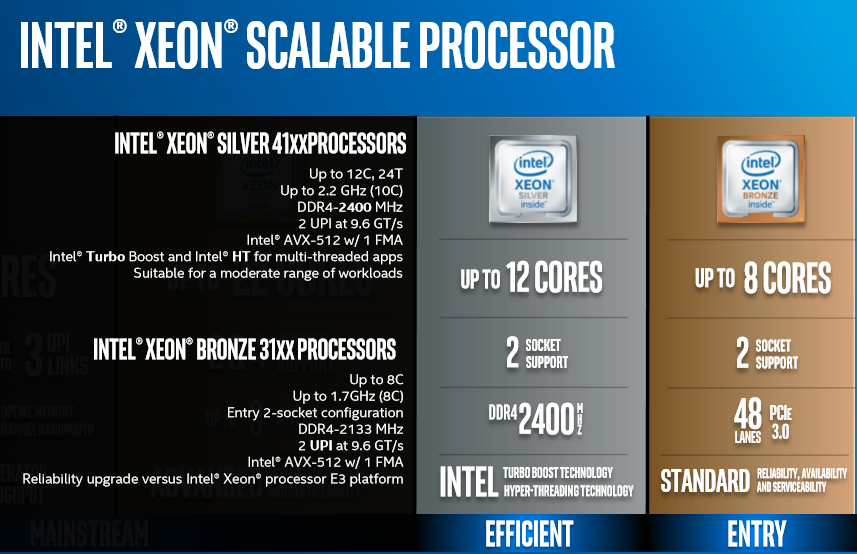
As with the Gold 5100 series, these Silver and Bronze parts only have 1 FMA per core for the AVX-512. The Silver parts support DDR4-2400, hyperthreading, and UPI at 9.6 GT/s (down from 10.4 GT/s on Gold), compared to the Bronze CPUs that use DDR4-2133, no hyperthreading, the slower UPI, but also slower in general – peak frequencies are at 1.7 GHz with AVX-512 at 0.8 GHz.
| Intel Xeon Skylake-SP Silver and Bronze Series | ||||||||||
| Segment | Cores | Base (GHz) |
Turbo (GHz) |
L3 (MB) |
L3/core (MB) |
TDP (W) |
Price (USD) |
|||
| 4116 | Perf/Watt | 12 | 2.1 | 3.0 | 16.50 | 1.375 | 85 | $1002 | ||
| 4116 | T | 10yr Life | 12 | 2.1 | 3.0 | 16.50 | 1.375 | 85 | $1112 | |
| 4114 | Perf/Watt | 10 | 2.2 | 3.0 | 13.75 | 1.375 | 85 | $694 | ||
| 4114 | T | 10yr Life | 10 | 2.2 | 3.0 | 13.75 | 1.375 | 85 | $773 | |
| 4112 | Perf/Watt | 4 | 2.6 | 3.0 | 5.50 | 1.375 | 85 | $473 | ||
| 4110 | Perf/Watt | 8 | 2.1 | 3.0 | 11.00 | 1.375 | 85 | $501 | ||
| 4109 | T | 10yr Life | 8 | 2.0 | 3.0 | 11.00 | 1.375 | 70 | $501 | |
| 4108 | Perf/Watt | 8 | 1.8 | 3.0 | 11.00 | 1.375 | 85 | $417 | ||
| 3106 | Perf/Watt | 8 | 1.7 | - | 11.00 | 1.375 | 85 | $306 | ||
| 3104 | Perf/Watt | 6 | 1.7 | - | 8.25 | 1.375 | 85 | $213 | ||
Overview
It is worth noting that Intel’s documents, such as the price lists do not list these parts in numerical order. At times the higher core count part will be listed higher than a lower core count part with more cache/frequency, and this will be non-obvious, especially when quick glancing. In general, the higher the number, the higher the raw performance is (Cores, frequency), but this does not always hold true.
The Platinum 8170 (165W) has only 2 cores (8%, 26 vs 24) more than the 8168 (205W), but the latter has an almost 30% higher frequency (2.7 vs 2.1). So maybe the higher the number, the better the performance/watt? This doesn’t hold either, because the 8164 (150W) runs 26 cores at a 2 GHz. The Gold 6144 and 6142 look very similar, but the former is an 8-core at 3.5 GHz (with 25 MB of L3), while the latter is a 16-core at 2.6 GHz (with 22 MB L3).
The new numbering and grade scheme has some merits, but there are still too many exceptions to rely on it. Especially the Gold grade having two sets of parts, and the last two numbers are not logical at all. You will still need to decipher every SKU at ark.intel.com to know what you are buying.


219 Comments
View All Comments
psychobriggsy - Tuesday, July 11, 2017 - link
Indeed it is a ridiculous comment, and puts the earlier crying about the older Ubuntu and GCC into context - just an Intel Fanboy.In fact Intel's core architecture is older, and GCC has been tweaked a lot for it over the years - a slightly old GCC might not get the best out of Skylake, but it will get a lot. Zen is a new core, and GCC has only recently got optimisations for it.
EasyListening - Wednesday, July 12, 2017 - link
I thought he was joking, but I didn't find it funny. So dumb.... makes me sad.blublub - Tuesday, July 11, 2017 - link
I kinda miss Infinity Fabric on my Haswell CPU and it seems to only have on die - so why is that missing on Haswell wehen Ryzen is an exact copy?blublub - Tuesday, July 11, 2017 - link
Your actually sound similar to JuanRGA at SAKevin G - Wednesday, July 12, 2017 - link
@CajunArson The cache hierarchy is radically different between these designs as well as the port arrangement for dispatch. Scheduling on Ryzen is split between execution resources where as Intel favors a unified approach.bill.rookard - Tuesday, July 11, 2017 - link
Well, that is something that could be figured out if they (anandtech) had more time with the servers. Remember, they only had a week with the AMD system, and much like many of the games and such, optimizing is a matter of run test, measure, examine results, tweak settings, rinse and repeat. Considering one of the tests took 4 hours to run, having only a week to do this testing means much of the optimization is probably left out.They went with a 'generic' set of relative optimizations in the interest of time, and these are the (very interesting) results.
CoachAub - Wednesday, July 12, 2017 - link
Benchmarks just need to be run on as level as a field as possible. Intel has controlled the market so long, software leans their way. Who was optimizing for Opteron chips in 2016-17? ;)theeldest - Tuesday, July 11, 2017 - link
The compiler used isn't meant to be the the most optimized, but instead it's trying to be representative of actual customer workloads.Most customer applications in normal datacenters (not google, aws, azure, etc) are running binaries that are many years behind on optimizations.
So, yes, they can get better performance. But using those optimizations is not representative of the market they're trying to show numbers for.
CajunArson - Tuesday, July 11, 2017 - link
That might make a tiny bit of sense if most of the benchmarks run were real-world workloads and not C-Ray or POV-Ray.The most real-world benchmark in the whole setup was the database benchmark.
coder543 - Tuesday, July 11, 2017 - link
The one benchmark that favors Intel is the "most real-world"? Absolutely, I want AnandTech to do further testing, but your comments do not sound unbiased.