Sizing Up Servers: Intel's Skylake-SP Xeon versus AMD's EPYC 7000 - The Server CPU Battle of the Decade?
by Johan De Gelas & Ian Cutress on July 11, 2017 12:15 PM EST- Posted in
- CPUs
- AMD
- Intel
- Xeon
- Enterprise
- Skylake
- Zen
- Naples
- Skylake-SP
- EPYC
AMD's EPYC Server CPU
If you have read Ian's articles about Zen and EPYC in detail, you can skip this page. For those of you who need a refresher, let us quickly review what AMD is offering.
The basic building block of EPYC and Ryzen is the CPU Complex (CCX), which consists of 4 vastly improved "Zen" cores, connected to an L3-cache. In a full configuration each core technically has its own 2 MB of L3, but access to the other 6 MB is rather speedy. Within a CCX we measured 13 ns to access the first 2 MB, and 15 to 19 ns for the rest of the 8 MB L3-cache, a difference that's hardly noticeable in the grand scheme of things. The L3-cache acts as a mostly exclusive victim cache.
Two CCXes make up one Zeppelin die. A custom fabric – AMD's Infinity Fabric – ties together two CCXes, the two 8 MB L3-caches, 2 DDR4-channels, and the integrated PCIe lanes. That topology is not without some drawbacks though: it means that there are two separate 8 MB L3 caches instead of one single 16 MB LLC. This has all kinds of consequences. For example the prefetchers of each core make sure that data of the L3 is brought into the L1 when it is needed. Meanwhile each CCX has its own separate (not inside the L3, so no capacity hit) and dedicated SRAM snoop directory (keeping track of 7 possible states). In other words, the local L3-cache communicates very quickly with everything inside the same CCX, but every data exchange between two CCXes comes with a tangible latency penalty.
Moving further up the chain, the complete EPYC chip is a Multi Chip Module(MCM) containing 4 Zeppelin dies.
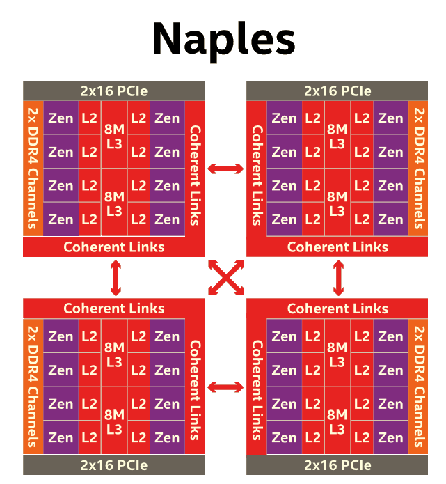
AMD made sure that each die is only one hop apart from the other, ensuring that the off-die latency is as low as reasonably possible.
Meanwhile scaling things up to their logical conclusion, we have 2P configurations. A dual socket EPYC setup is in fact a "virtual octal socket" NUMA system.

AMD gave this "virtual octal socket" topology ample bandwidth to communicate. The two physical sockets are connected by four bidirectional interconnects, each consisting of 16 PCIe lanes. Each of these interconnect links operates at +/- 38 GB/s (or 19 GB/s in each direction).
So basically, AMD's topology is ideal for applications with many independently working threads such as small VMs, HPC applications, and so on. It is less suited for applications that require a lot of data synchronization such as transactional databases. In the latter case, the extra latency of exchanging data between dies and even CCX is going to have an impact relative to a traditional monolithic design.


219 Comments
View All Comments
alpha754293 - Tuesday, July 11, 2017 - link
Pity that OpenFOAM failed to run on Ubuntu 16.04.2 LTS. I would have been very interested in those results.farmergann - Tuesday, July 11, 2017 - link
Are you trying to hide the fact that AMD's performance per watt absolutely dominates intel's, or have you simply overlooked one of, if not the, single most important aspects of server processors?Ryan Smith - Tuesday, July 11, 2017 - link
Neither. We just had very little time to look at power consumption. It's also the metric we're the least confident in right now, as we'd like to have a better understanding of the quirks of the platform (which again takes more time).Carl Bicknell - Wednesday, July 12, 2017 - link
Ryan / Ian,Just to let you know there are better chess benchmarks than the one you've chosen. Stockfish is an example of a newer program which better uses modern CPU architecture.
NixZero - Tuesday, July 11, 2017 - link
"AMD's MCM approach is much cheaper to manufacture. Peak memory bandwidth and capacity is quite a bit higher with 4 dies and 2 memory channels per die. However, there is no central last level cache that can perform low latency data coordination between the L2-caches of the different cores (except inside one CCX). The eight 8 MB L3-caches acts like - relatively low latency - spill over caches for the 32 L2-caches on one chip. "isnt skylake-x's l3 a victim cache too? and divided at 1.3mb for each core, not a monolytic one?
Ian Cutress - Tuesday, July 11, 2017 - link
That's what a 'spill-over' cache is - it accepts evicted cache lines.NixZero - Wednesday, July 12, 2017 - link
so why its put as an advantage for intel cache, which is spill over too?JonathanWoodruff - Wednesday, July 12, 2017 - link
Since the Intel one is all on one die, a miss to a "slice" of cache can be filled without DRAM-like latencies from another slice. Since AMD has it's last level caches spread across dies, going to another cache looks to be equivalent latency-wise to going to DRAM. It wouldn't necessarily have to be quite that bad, and I would expect some improvement here for Zen2.Martin_Schou - Tuesday, July 11, 2017 - link
This has to be wrong:CPU Two EPYC 7601 (2.2 GHz, 32c, 8x8MB L3, 180W)
RAM 512 GB (12x32 GB) Samsung DDR4-2666 @2400
12 x 32 GB is 384 GB, and 12 sticks doesn't fit nicely into 8 channels. In all likelihood that's supposed to be 16x32 GB, as we see in the E52690
Dr.Neale - Tuesday, July 11, 2017 - link
I find myself puzzled by the curious omission in this article of a key aspect of Server architecture: Data Security.AMD has a LOT; Intel, not so much.
I would think this aspect of Server "Performance" would be a major consideration in choosing which company's Architecture to deploy in a Secure Server scenario. Especially in light of Recent Revelations fuelling Hacking Headlines in the news, and Dominating Discussions on various social media websites.
How much is Data Security worth?
A topic of EPYC consequence!