Sizing Up Servers: Intel's Skylake-SP Xeon versus AMD's EPYC 7000 - The Server CPU Battle of the Decade?
by Johan De Gelas & Ian Cutress on July 11, 2017 12:15 PM EST- Posted in
- CPUs
- AMD
- Intel
- Xeon
- Enterprise
- Skylake
- Zen
- Naples
- Skylake-SP
- EPYC
Intel's New On-Chip Topology: A Mesh
Since the introduction of the "Nehalem" CPU architecture – and the Xeon 5500 that started almost a decade-long reign for Intel in the datacenter – Intel's engineers have relied upon a low latency, high bandwidth ring to connect their cores with their caches, memory controllers, and I/O controllers.
Intel's most recent adjustment to their ring topology came with the Ivy Bridge-EP (Xeon E5 2600 v2) family of CPUs. The top models were the first with three columns of cores connected by a dual ring bus, which utilized both outer and inner rings. The rings moved data in opposite directions (clockwise/counter-clockwise) in order to minimize latency by allowing data to take the shortest path to the destination. As data is brought onto the ring infrastructure, it must be scheduled so that it does not collide with previous data.
The ring topology had a lot of advantages. It ran very fast, up to 3 GHz. As result, the L3-cache latency was pretty low: if the core is lucky enough to find the data in its own cache slice, only one extra cycle is needed (on top of the normal L1-L2-L3 latency). Getting a cacheline of another slice can cost up to 12 cycles, with an average cost of 6 cycles.
However the ring model started show its limits on the high core count versions of the Xeon E5 v3, which had no less than four columns of cores and LLC slices, making scheduling very complicated: Intel had to segregate the dual ring buses and integrate buffered switches. Keeping cache coherency performant also became more and more complex: some applications gained quite a bit of performance by choosing the right snoop filter mode (or alternatively, lost a lot of performance if they didn't pick the right mode). For example, our OpenFOAM benchmark performance improved by almost 20% by choosing "Home Snoop" mode, while many easy to scale, compute-intensive applications preferred "Cluster On Die" snooping mode.
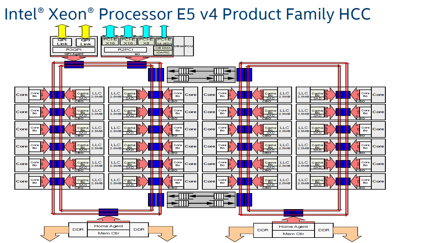
In other words, placing 22 (E7:24) cores, several PCIe controllers, and several memory controllers was close to the limit what a dual ring could support. In order to support an even larger number of cores than the Xeon v4 family, Intel would have to add a third ring, and ultimately connecting 3 rings with 6 columns of cores each would be overly complex.
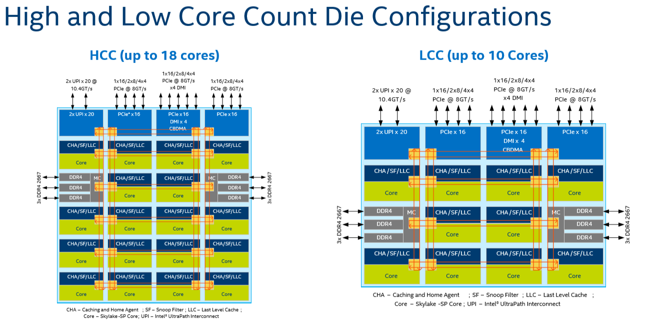
Given that, it shouldn't come as a surprise that Intel's engineers decided to use a different topology for Skylake-SP to connect up to 28 cores with the "uncore." Intel's new solution? A mesh architecture.
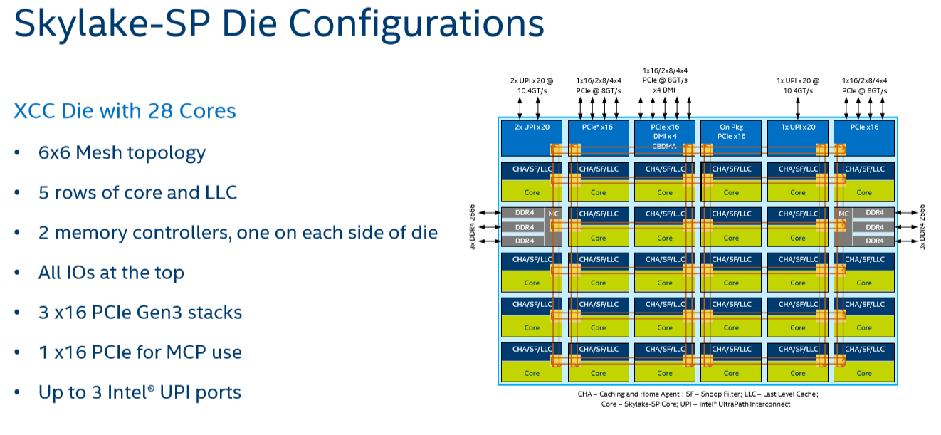
Under Intel's new topology, each node – a caching/home agent, a core, and a chunk of LLC – is interconnected via a mesh. Conceptually it is very similar to the mesh found on Xeon Phi, but not quite the same. In the long-run the mesh is far more scalable than Intel's previous ring topology, allowing Intel to connect many more nodes in the future.
How does it compare to the ring architecture? The Ring could run at up to 3 GHz, while the current mesh and L3-cache runs at at between 1.8GHZ and 2.4GHz. On top of that, the mesh inside the top Skylake-SP SKUs has to support more cores, which further increases the latency. Still, according to Intel the average latency to the L3-cache is only 10% higher, and the power usage is lower.
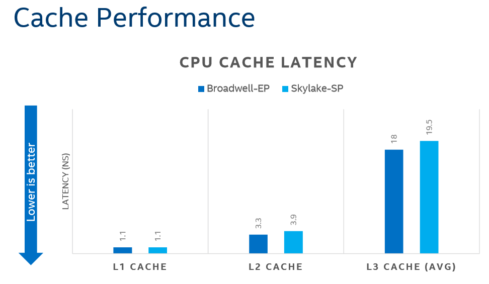
A core that access an L3-cache slice that is very close (like the ones vertically above each other) gets an additional latency of 1 cycle per hop. An access to a cache slice that is vertically 2 hops away needs 2 cycles, and one that is 2 hops away horizontally needs 3 cycles. A core from the bottom that needs to access a cache slice at the top needs only 4 cycles. Horizontally, you get a latency of 9 cycles at the most. So despite the fact that this Mesh connects 6 extra cores verse Broadwell-EP, it delivers an average latency in the same ballpark (even slightly better) as the former's dual ring architecture with 22 cores (6 cycles average).
Meanwhile the worst case scenario – getting data from the right top node to the bottom left node – should demand around 13 cycles. And before you get too concerned with that number, keep in mind that it compares very favorably with any off die communication that has to happen between different dies in (AMD's) Multi Chip Module (MCM), with the Skylake-SP's latency being around one-tenth of EPYC's. It is crystal clear that there will be some situations where Intel's server chip scales better than AMD's solution.
There are other advantages that help Intel's mesh scale: for example, caching and home agents are now distributed, with each core getting one. This reduces snoop traffic and reduces snoop latency. Also, the number of snoop modes is reduced: no longer do you need to choose between home snoop or early snoop. A "cluster-on-die" mode is still supported: it is now called sub-NUMA Cluster or SNC. With SNC you can divide the huge Intel server chips into two NUMA domains to lower the latency of the LLC (but potentially reduce the hitrate) and limit the snoop broadcasts to one SNC domain.


219 Comments
View All Comments
TheOriginalTyan - Tuesday, July 11, 2017 - link
Another nicely written article. This is going to be a very interesting next couple of months.coder543 - Tuesday, July 11, 2017 - link
I'm curious about the database benchmarks. It sounds like the database is tiny enough to fit into L3? That seems like a... poor benchmark. Real world databases are gigabytes _at best_, and AMD's higher DRAM bandwidth would likely play to their favor in that scenario. It would be interesting to see different sizes of transactional databases tested, as well as some NoSQL databases.psychobriggsy - Tuesday, July 11, 2017 - link
I wrote stuff about the active part of a larger database, but someone's put a terrible spam blocker on the comments system.Regardless, if you're buying 64C systems to run a DB on, you likely will have a dataset larger than L3, likely using a lot of the actual RAM in the system.
roybotnik - Wednesday, July 12, 2017 - link
Yea... we use about 120GB of RAM on the production DB that runs our primary user-facing app. The benchmark here is useless.haplo602 - Thursday, July 13, 2017 - link
I do hope they elaborate on the DB benchmarks a bit more or do a separate article on it. Since this is a CPU article, I can see the point of using a small DB to fit into the cache, however that is useless as an actual DB test. It's more an int/IO test.I'd love to see a larger DB tested that can fit into the DRAM but is larger than available caches (32GB maybe ?).
ddriver - Tuesday, July 11, 2017 - link
We don't care about real world workloads here. We care about making intel look good. Well... at this point it is pretty much damage control. So let's lie to people that intel is at least better in one thing.Let me guess, the databse size was carefully chosen to NOT fit in a ryzen module's cache, but small enough to fit in intel's monolithic die cache?
Brought to you by the self proclaimed "Most Trusted in Tech Since 1997" LOL
Ian Cutress - Tuesday, July 11, 2017 - link
I'm getting tweets saying this is a severely pro AMD piece. You are saying it's anti-AMD. ¯\_(ツ)_/¯ddriver - Tuesday, July 11, 2017 - link
Well, it is hard to please intel fanboys regardless of how much bias you give intel, considering the numbers.I did not see you deny my guess on the database size, so presumably it is correct then?
ddriver - Tuesday, July 11, 2017 - link
In the multicore 464.h264ref test we have 2670 vs 2680 for the xeon and epyc respectively. Considering that the epyc score is mathematically higher, howdoes it yield a negative zero?Granted, the difference is a mere 0.3% advantage for epyc, but it is still a positive number.
Headley - Friday, July 14, 2017 - link
I thought the exact same thing