Exploring DynamIQ and ARM’s New CPUs: Cortex-A75, Cortex-A55
by Matt Humrick on May 29, 2017 12:00 AM EST- Posted in
- Smartphones
- CPUs
- Arm
- Mobile
- Cortex
- DynamIQ
- Cortex A75
- Cortex A55
Cortex-A55 Microarchitecture
The Cortex-A55 is the next CPU microarchitecture in ARM’s Cambridge family of low-power, small-footprint cores, which also include the A5, A7, and A53. This new little core is an evolution of the A53, so the two cores share much in common. Using the A53 as the starting point makes sense—it has proven to be a successful design—but as the big cores evolved over time, the performance gap between the big cores and the A53 grew, altering the balance in ARM’s big.LITTLE scheme. And as ARM continues its push into new markets beyond mobile, it needs new features that the A53 lacks. The A55 addresses the performance issue with improvements to the memory system and other microarchitectural changes and adds key features by moving from the ARMv8.0 architecture to ARMv8.2.
At a high level, the A55 is still a dual-issue, in-order CPU with an 8-stage pipeline. According to ARM, 8 stages is still the sweet spot, because it’s not seeing significant frequency improvements when moving from 16/14nm to 10nm to 7nm (most of the process gains are with area scaling and reduced dynamic/leakage power). With 8 stages, the A55 should reach a similar peak frequency as A53. Moving to a shorter pipeline would reduce the max frequency without a significant improvement to power or area, while a longer pipeline would increase area and power consumption for only a small frequency gain.
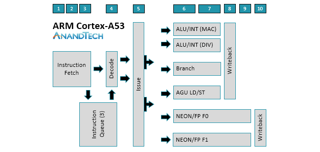
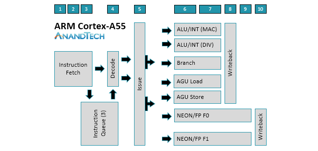
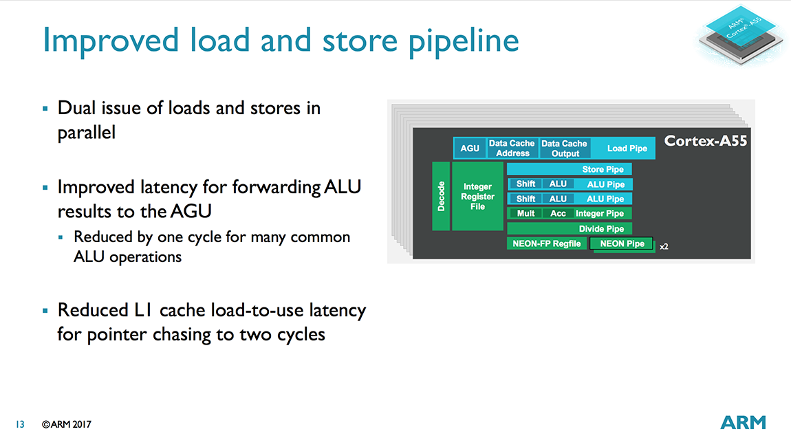
The similarities between the two cores is evident when examining the diagrams above. There’s still a 2-wide decode stage that decodes most instructions in a single cycle. Another feature that carries over from A53 is symmetric dual-issue for most instructions, meaning both issue slots can feed instructions to any pipeline. We’ll cover the execution pipelines in more detail below, but the big change here is that the A55 moves to independent load and store AGUs that can perform loads and stores in parallel instead of a single, combined AGU like the A53.
The A53’s core already provides good throughput, but not having instructions or data ready to process, perhaps because of a mispredicted branch or a cache miss, nullifies this advantage. Without the ability to execute instructions out of order while the CPU waits to fetch an instruction or data from elsewhere in the memory hierarchy, the entire core can stall (all other instructions need to wait for the current instruction to finish), so keeping an in-order core fed with instructions and data is critical. This is why ARM focused heavily on improving the A55’s memory system performance.
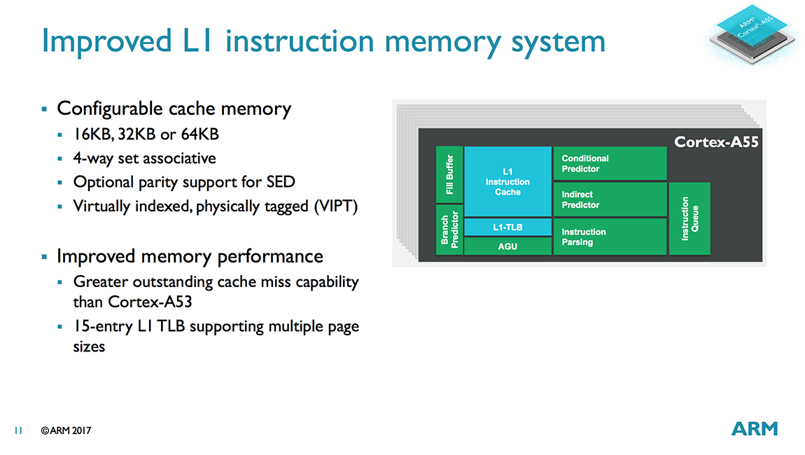
Starting on the instruction side, the L1 I-cache is now 4-way set associative versus 2-way for the A53. It’s still VIPT (Virtually Indexed, Physically Tagged), which is commonly used for L1 caches as it reduces latency, but there’s a larger 15-entry L1 TLB that supports multiple page sizes. This simple-sounding change actually required a significant amount of work to alleviate issues with timing pressure. The size of the L1 I-cache is configurable with options for 16KB, 32KB, or 64KB, which is similar to the A53 that offers a range from 8KB to 64KB.
It seems that every new CPU microarchitecture comes with a new branch predictor, and the A55 is no exception. The new conditional predictor increases prediction accuracy by using neural network based algorithms. It also adds loop termination prediction, which avoids a mispredict occurring at the end of a loop. There are also new 0-cycle micro-predictors ahead of the main conditional predictor. These are not as accurate as the main predictor, but their ability to perform predictions back to back to back provide a significant performance uplift by reducing pipeline bubbles even in tight loops. There’s also an indirect predictor that’s only used when necessary, reducing the power penalty because indirect branches do not occur as frequently. This includes a 256-entry BTAC (Branch Target Address Cache).
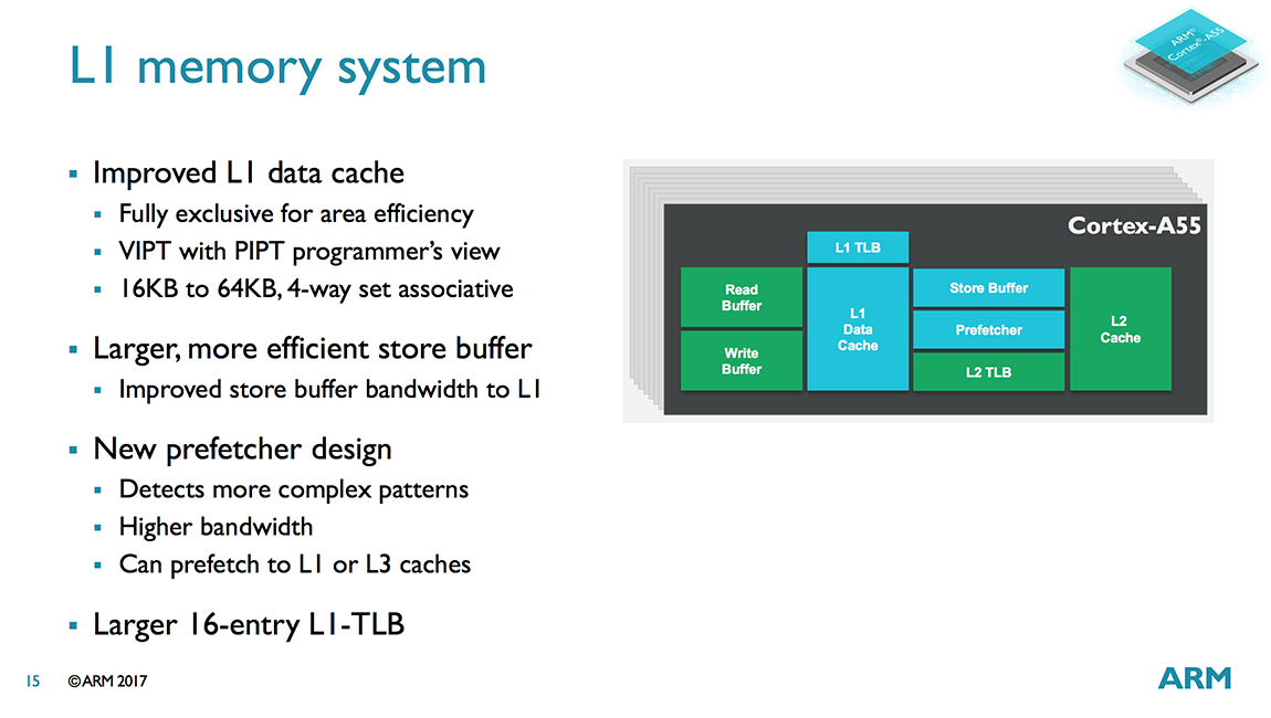
Switching over to the data path, the A55 includes an improved data prefetcher that delivers higher bandwidth. It’s capable of detecting more complex cache miss patterns and can prefetch to the L1 or L3 caches. ARM expects these improvements to make a noticeable impact on mobile device UI performance.
The L1 D-cache is still 4-way set associative like the A53, but is now fully-exclusive instead of pseudo-exclusive, which saves area because data is not duplicated in the L2 cache. The size of the L1 D-cache is also configurable with 16KB, 32KB, or 64KB options, which is also similar to the A53’s range from 8KB to 64KB.
Another big change for the L1 D-cache is moving from a PIPT (Physically Indexed, Physically Tagged) to a VIPT access scheme. This reduces cache latency because the cache index lookup happens in parallel with the TLB translation, but also creates aliasing issues where several virtual addresses might reference the same physical address. The A55 deals with aliasing in hardware, however, making the VIPT cache appear like a PIPT cache to the programmer.
Further enhancements include a larger 16-entry micro-TLB for the L1 D-cache, a significant increase over the A53’s 10-entry micro-TLB, and a larger store buffer with higher bandwidth into the L1 to better cope with workloads that generate a lot of stores. ARM also reduced the L1 pointer chasing load-to-use latency from 3 cycles in A53 to 2 cycles in A55, providing a small performance bump when working with certain types of data structures.
Being compatible with DynamIQ means the A55 gets an integrated L2 cache that operates at core speed. This reduces L2 latency by 50% (12 cycles to 6 cycles) compared to the A53 and its shared L2. The L2 cache size options include 0KB, 64KB, 128KB, and 256KB. ARM expects 128KB to be the most common for mobile applications, but there should be a reasonable number of 256KB configurations too. The smaller sizes will appeal to the networking and embedded markets that desire lower area/cost or need more deterministic memory behavior. With the L2 now part of the core, the A55’s L2 TLB grows to 1024 entries up from 512 entries for A53.
The A55’s integrated L2 uses PIPT, which is simpler to implement and uses less power than VIPT. Unlike the VIPT L1, using PIPT for the L2 does not incur a performance penalty because its naturally higher latency means there’s sufficient time to get the physical address from the TLB before performing the tag compare.
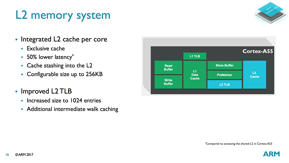
The L2 is 4-way set associative like the L1, a design choice meant to minimize cache latency, which is important for reducing the impact of stalls on in-order cores. The downside to using a less associative cache is a greater chance to miss, but ARM feels comfortable with this compromise with an L3 cache sitting reasonably close to the core.
Having access to a (potentially) large L3 cache, something the A53 did not have, will also help improve performance. As previously stated, in-order cores are sensitive to cache misses that cause the core to stall, so they respond particularly well to increases in cache size and reductions in memory access latency. ARM says the A53/A55 sees roughly a 5% performance improvement for each doubling of cache size depending on workload.
We’ll end our tour through the data path and our discussion about the A55’s memory system improvements with the AGUs (Address Generation Units). According to ARM’s internal benchmarking, the CPU can spend a lot of time doing loads and stores, so improving performance here was crucial. Instead of sticking with the A53’s single, combined AGU, the A55 uses independent load and store AGUs that can perform loads and stores in parallel, enabling a higher issue rate into the memory system. Note that the A55’s AGUs are not capable of performing both loads and stores (just one or the other) like the AGUs in the A73/A75, a trade off between performance and complexity.
Shifting our focus to the execution pipes, we find 2 ALU/INT units that are functionally the same as the A53’s. Both ALUs can perform basic operations such as additions and shifts, but only one ALU handles integer multiplication and multiply-accumulate operations, while the other focuses on integer division with a Radix-16 divider. So while the A53/A55 cannot perform 2 integer multiplies or divides in parallel, it can dual issue a MUL/MAC alongside a divide/add/shift. The ALUs are still 2 stages, but nearly all instructions complete in 1 cycle. There are also several forwarding paths built in, including paths within the same pipe or cross pipe, to reduce execution latency.
The 2 64-bit NEON/Floating Point pipes are still optional (some markets do not require them) and are served from a dedicated 128-bit register file like the A53. Each SIMD NEON pipe in the A53/A55 can perform 8 8-bit integer, 4 16-bit integer, 2 32-bit integer or single-precision floating-point (FP), or 1 64-bit integer or double-precision FP operations per cycle, giving programmers the flexibility to choose the right balance between precision and performance. As part of its support for the ARMv8.2 architecture, the A55 gains native support for half-precision FP16 operations too. The A53 can fetch FP16 values, but they need to be converted to FP32 before execution. This is no longer the case with A55, so the core performs less work when dealing with FP16 values that are frequently used in some image processing and machine learning applications that require 16-bit precision.
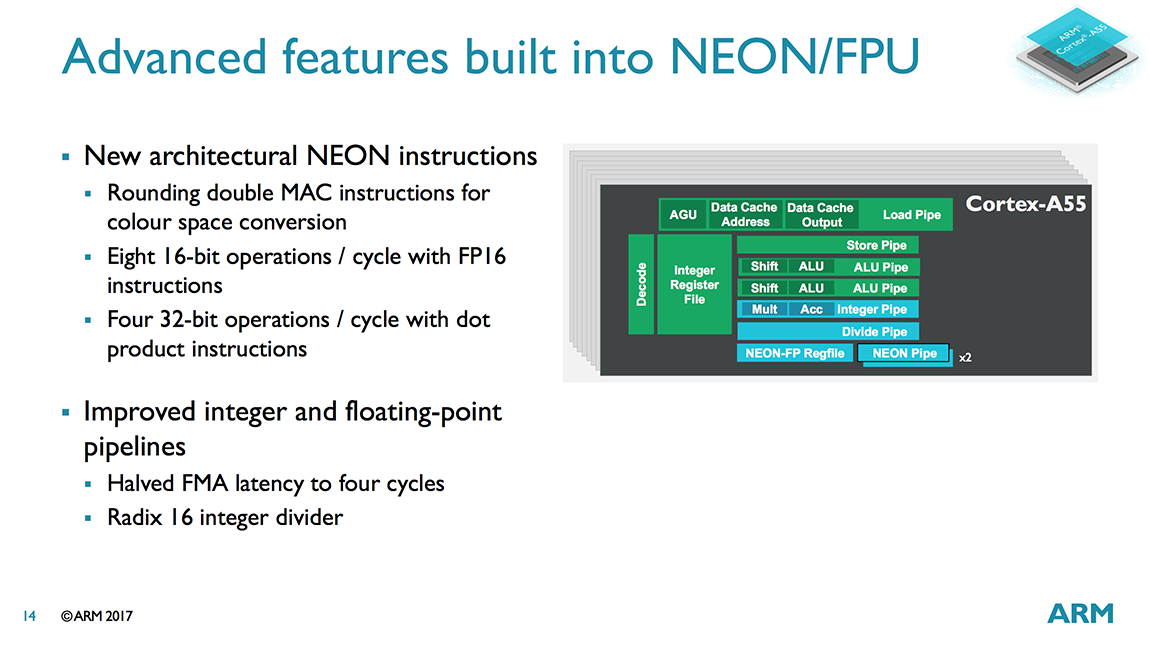
The A55 also includes a new INT8 dot product instruction, another useful addition for machine learning, that offers a 4x performance improvement over the A53 (which increases to about 5x when taking the memory system improvements into account). Instead of executing multiple instructions back to back to back like the A53, the A55 only needs to push a single instruction through the pipe.
One final noteworthy improvement is the ability to do a fused multiply–add (FMA) in a single pass instead of two for the A53, reducing latency from 8 cycles to 4.
The A55 has much in common with the A53, which is not surprising because the A53 already delivers good core throughput. While the A55 gets some improvements to the NEON/FP pipes, mostly from additional instructions courtesy of ARMv8.2, most of its performance gains come from changes to the memory system meant to reduce both the number of core stalls and their latency impact when they do occur.


104 Comments
View All Comments
Wilco1 - Tuesday, May 30, 2017 - link
All of the Helio deca cores use Cortex-A72, just like Snapdragon 65x, and the higher clocks of Helio means it beats the 65x like you'd expect. So I'm not sure what your point is?Cortex-A53 in Kirin 950 at its highest frequency is ~50% more efficient than Cortex-A72, with the crossover point at around 2.1GHz. On 10nm with Cortex-A55 it may be closer to 2.5GHz.
serendip - Tuesday, May 30, 2017 - link
Yeah, my mistake, I was thinking of Helios with 8x A53s only. Anyway, perf/watt matters at high clock speeds, so a 50% efficient A53 still can't do as much work as an A72 at the same clock speed. I'd rather keep the efficient cores humming along at low speed and have the big cores come online in short bursts, like for app loading or web page rendering. Note that this might not work for constant gaming though, the big cores constantly being on will overheat the phone and kill battery life.No easy solutions then.
Wardrive86 - Tuesday, May 30, 2017 - link
2 GHz a53 has the single thread performance of 2.3 GHz Krait 400/1.85 GHz cortex a15. Octa designs often have well over double the multithread performance of say a Snapdragon 800/801. Not low end..very much midrangeserendip - Tuesday, May 30, 2017 - link
But the A53 or A55 at 2+ GHz is a huge power hog that's still slower than a similarly clocked A72 or A75. The octacore branding is a gimmick when all cores are the same design. Performance doesn't scale equally with increasing frequency and power consumption - at one point, it's better to switch the task to a high performance core rather than keep increasing speed on a low performance core.A smart design (like the 650/652 which is a flagship killer) would 4x or 6x A55 at low clock rates for multi threaded stuff and 2x A75 for pure single threaded performance, power consumption be damned.
Wardrive86 - Tuesday, May 30, 2017 - link
Snapdragon 625 @ 2.02 GHz and 626 @ 2.3 GHz are certainly not battery hogs. They are both homogenous and ramp clock speed up on all cores very, very often. Much snappier performance than paper specs would suggest and incredible battery lifeStrangerGuy - Tuesday, May 30, 2017 - link
Midrange ARM big cores at actual midrange prices are already quite a rarity in the China phone market, let alone outside of it. Since they perform so close to actual flagships SoCs, most OEMs will either price the devices similarly to their actual flagships (cough Samsung A9 Pro), or not doing them altogether. If you ask me who to blame, it will be the non-Apple custom core designers sucking hard at their jobs.Besides an A55 SoC with presumably >1K ST GB4 scores are no slouches either, for a $120 device I'm certainly not complaining.
serendip - Friday, June 2, 2017 - link
Maybe the 650/652 was a flash in the pan and the 660 could be a unicorn chip, one that's announced but never deployed. Interestingly Xiaomi moved to the 625 in the Redmi Note 4 and Mi Max 2, whereas predecessor models used the 650. Maybe OEMs really are afraid of good-enough chips in their midrange devices cannibalizing flagship sales.legume - Tuesday, May 30, 2017 - link
All of these numbers are crap if the cache configs are not stated. DynamIQ is very different and most of the SPEC gains could be from L2/LLC increases. This is all marketing FUDWilco1 - Tuesday, May 30, 2017 - link
Forgot to read the article?"These numbers, as well as the others shown in the chart, comparing the A55 and A53 are at the same frequency, same L1/L2 cache sizes, same compiler, etc. and are meant to be a fair comparison. The actual gains should actually be a little higher, because partner SoCs will benefit from adding the L3 cache, which these numbers do not include."
legume - Wednesday, May 31, 2017 - link
iso is not the same as knowing the values