Samsung and TSMC Roadmaps: 8 and 6 nm Added, Looking at 22ULP and 12FFC
by Anton Shilov on May 5, 2017 9:30 AM ESTBeyond 10 nm at Samsung: 8 nm and 6 nm
Samsung’s 7 nm manufacturing technology is still expected to be the company’s first process to use extreme ultraviolet lithography (EUVL) for high-volume manufacturing (HVM) and that is going to happen sometimes in 2019 or later (risk production starts in the second half of 2018). In fact, the next several years down the road is where things will start to get interesting as Samsung announced another two new production technologies it has not talked about before: the 8 nm and the 6 nm processes.
| Industry FinFET Lithography Roadmap, HVM Start Data announced by companies during conference calls, press briefings and in press releases |
||||||||||||
| 2016 | 2017 | 2018 | 2019 | 2020 | 2021 | |||||||
| 1H | 2H | 1H | 2H | 1H | 2H | 1H | 2H | |||||
| GlobalFoundries | 14LPP | 7nm DUV | 7nm with EUV* | |||||||||
| Intel | 14 nm 14 nm+ |
14 nm++ 10 nm |
10 nm+ 10 nm++ |
|||||||||
| Samsung | 14LPP 14LPC |
10LPE | 10LPP | 8LPP 10LPU |
7LPP | 6 nm* (?) | ||||||
| SMIC | 28 nm** | 14 nm in development | ||||||||||
| TSMC | CLN16FF+ CLN16FFC | CLN10FF CLN16FFC |
CLN7FF CLN12FFC |
CLN12FFC/ CLN12ULP |
CLN7FF+ | 5 nm* (?) | ||||||
| UMC | 28 nm** | 14nm | no data | |||||||||
| *Exact timing not announced **Planar |
||||||||||||
Officially, Samsung says that both technologies will offer “greater scalability, performance and power advantages when compared to existing process nodes,” which obviously means that they are across the board better than Samsung’s current-gen 14 nm and 10 nm offerings. What is important is that Samsung also says that the “8 nm and the 6 nm will inherit all innovations from the latest 10 nm and the 7 nm technologies” respectively. This means that the 8 nm is set to keep using DUV and multi patterning (triple patterning or even quad patterning to be exact, but Samsung has not confirmed usage of the latter) for critical layers, whereas the 6 nm will come after 7 nm and will be Samsung’s second-generation EUV technology.
The only thing that Samsung confirms about its 8LPP manufacturing technology right now is the fact that this is a DUV-based process technology designed to shrink die size (i.e., increase transistor density) and frequency compared to the 10LPP fabrication process. Given the name of the technology and its key advertised advantages over direct predecessor, it is highly likely that the 8LPP will be used to make high-performance SoCs in 2019.
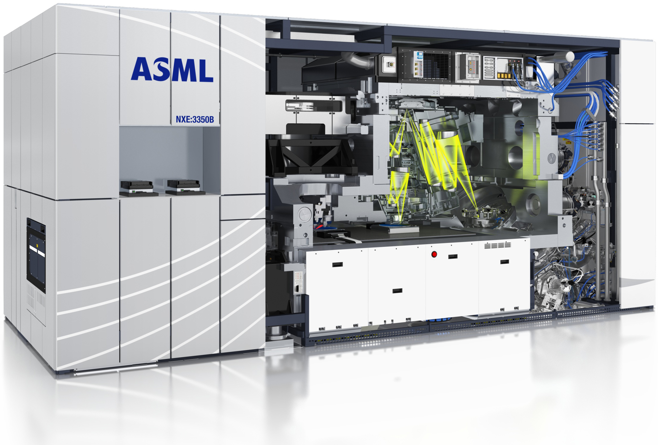
Since Samsung plans to start risk production using the 7LPP in the second half of 2018, the technology is hardly going to be used for high-volume manufacturing before the second half of 2019. Keeping in mind that Samsung now begins HVM using its leading-edge process technologies in October, it is possible that it is going to kick-off 7LPP HVM in fall 2019, but the 8LPP will be Samsung’s most advanced process technology for the better part of the year. Samsung does not mention timeframes for its 6 nm process technology and what to expect from it, but it is logical to assume that it will require more layers to be processed using ASML's EUV tools (like the NXE:3350B pictured above) in a bid to provide PPA advantages and it not be used for high-volume manufacturing before late 2020.
In March, Samsung only made brief announcements regarding its 10LPU, 8LPP and 6 nm process technology without disclosing their exact specifications or even PPA improvements targets. The addition of at least two more DUV technologies (the 10LPU and the 8LPP) in general may indicate that EUV may not be the best choice for all applications in 2019 – 2021, which is perfectly logical. Then again, we do not know how DUV and EUV technologies will co-exist early in the EUV era.
We are going to learn more about Samsung’s plans in the foundry industry in late May, when the company hosts its 2017 U.S Samsung Foundry Forum. So, we will have to wait for a couple of months for Samsung to disclose the whole picture regarding its upcoming process technologies.


89 Comments
View All Comments
SuperMecha - Saturday, May 6, 2017 - link
“First of all, neither he, or anyone else outside those companies actually knows enough about the actual chips to know the true density.”That’s grossly false. Their customers (i.e. AMD, Nvidia, Qualcomm, etc.) need to have the PDKs to design their chips. The PDKs will contain the design rules and ultimately the transistor specifications necessary to design a chip for that process. TSMC will be accepting 7nm tape outs this quarter which means the transistor specifications were likely frozen some time ago. Never mind the fact that the companies have released details of their future process nodes.
Wilco1 - Sunday, May 7, 2017 - link
I guess you also don't believe then that both TSMCs and GF's 16/14nm processes are already denser than Intel's 14nm? See eg. http://www.anandtech.com/show/11170/the-amd-zen-an... Apple A8 on 20nm was shown to be much denser than Core M on 14nm.Whatever the marketing claims say, Intel is already behind on density in actual designs. Intel's latest 14nm process is even less dense. So what makes you think that Intel could catch up?
melgross - Wednesday, May 10, 2017 - link
Because what you're saying is wrong. I haven't read anything saying that intels's process is less dense.Wilco1 - Thursday, May 11, 2017 - link
Well the link I provided shows it very clearly - I presume you didn't read it?Intel may have better CPP/MP/FP/SRAM at 14nm vs TSMC/GF, but AMD still gets better L2 and L3 density despite the less advanced process. And density on real designs matters more than the process marketing numbers (which are about bragging rights, but don't tell the whole story).
lefty2 - Sunday, May 7, 2017 - link
Scott's analysis was actually spot on. Dick James of TechInsights actually measured Samsungs 10nm chip: https://twitter.com/Siliconicsdick/status/85632866...measuring a 68 mm contacted gate pitch, 51 nm metal pitch, dual STI and single dummy gate.
That's compared to Intel's 14nm of 70 nm CPP x 52 nm MMP
By comparison: Intel's 14nm is 70 nm CPP x 52 nm MMP.
sc14s - Friday, May 5, 2017 - link
Seems to me past 2025 or so what are they going to do to compete assuming you hit that ~5nm and then iterate a few times on that process to maximize it's potential?You can't really go any further without some major physics breakthrough. it's kinda a race to the bottom just in a physics sense instead of the financial price slashing sense.
melgross - Friday, May 5, 2017 - link
Most of the work has been with carbon nanotubes, with both IBM and Hp showing progress. But it's not expected to go commercial (if ever, really) before the mid 2020s, or possibly (more likely), the later part of the decade.So there will be a gap. Software developers will need to improve their software to improve performance finally, which should be a big benefit for everything.
bji - Friday, May 5, 2017 - link
Regular hardware speed increases have allowed more software to be produced across a broader range of products more quickly because developers don't have to spend their time optimizing for performance as much because the hardware gets them to a 'good enough' place easily. Once the hardware is not getting faster, for every problem that requires greater performance, you simply shift more of the cost of creating the product to the software side. It will take longer to produce programs as a result. There is no free lunch; it's not like software development could have for no extra cost added more performance and now that hardware stops increasing in speed software development will just start adding that free performance in. The cost of producing software will just go up for that segment of the software market that is performance sensitive. Of course, quite a lot of the market is not performance sensitive so there will be little appreciable impact on most of the software market.tarqsharq - Friday, May 5, 2017 - link
It would be quite the time to be a skilled software developer though.A next generation John Carmack? Using computing tricks to pull off things that traditionally would bog down the available hardware?
vladx - Friday, May 5, 2017 - link
You're assuming that there are real solutions that could revolutionize software performance and scalability, just like the P versus NP problem we might never get an answer to that.