Samsung and TSMC Roadmaps: 8 and 6 nm Added, Looking at 22ULP and 12FFC
by Anton Shilov on May 5, 2017 9:30 AM ESTBeyond 10 nm at Samsung: 8 nm and 6 nm
Samsung’s 7 nm manufacturing technology is still expected to be the company’s first process to use extreme ultraviolet lithography (EUVL) for high-volume manufacturing (HVM) and that is going to happen sometimes in 2019 or later (risk production starts in the second half of 2018). In fact, the next several years down the road is where things will start to get interesting as Samsung announced another two new production technologies it has not talked about before: the 8 nm and the 6 nm processes.
| Industry FinFET Lithography Roadmap, HVM Start Data announced by companies during conference calls, press briefings and in press releases |
||||||||||||
| 2016 | 2017 | 2018 | 2019 | 2020 | 2021 | |||||||
| 1H | 2H | 1H | 2H | 1H | 2H | 1H | 2H | |||||
| GlobalFoundries | 14LPP | 7nm DUV | 7nm with EUV* | |||||||||
| Intel | 14 nm 14 nm+ |
14 nm++ 10 nm |
10 nm+ 10 nm++ |
|||||||||
| Samsung | 14LPP 14LPC |
10LPE | 10LPP | 8LPP 10LPU |
7LPP | 6 nm* (?) | ||||||
| SMIC | 28 nm** | 14 nm in development | ||||||||||
| TSMC | CLN16FF+ CLN16FFC | CLN10FF CLN16FFC |
CLN7FF CLN12FFC |
CLN12FFC/ CLN12ULP |
CLN7FF+ | 5 nm* (?) | ||||||
| UMC | 28 nm** | 14nm | no data | |||||||||
| *Exact timing not announced **Planar |
||||||||||||
Officially, Samsung says that both technologies will offer “greater scalability, performance and power advantages when compared to existing process nodes,” which obviously means that they are across the board better than Samsung’s current-gen 14 nm and 10 nm offerings. What is important is that Samsung also says that the “8 nm and the 6 nm will inherit all innovations from the latest 10 nm and the 7 nm technologies” respectively. This means that the 8 nm is set to keep using DUV and multi patterning (triple patterning or even quad patterning to be exact, but Samsung has not confirmed usage of the latter) for critical layers, whereas the 6 nm will come after 7 nm and will be Samsung’s second-generation EUV technology.
The only thing that Samsung confirms about its 8LPP manufacturing technology right now is the fact that this is a DUV-based process technology designed to shrink die size (i.e., increase transistor density) and frequency compared to the 10LPP fabrication process. Given the name of the technology and its key advertised advantages over direct predecessor, it is highly likely that the 8LPP will be used to make high-performance SoCs in 2019.
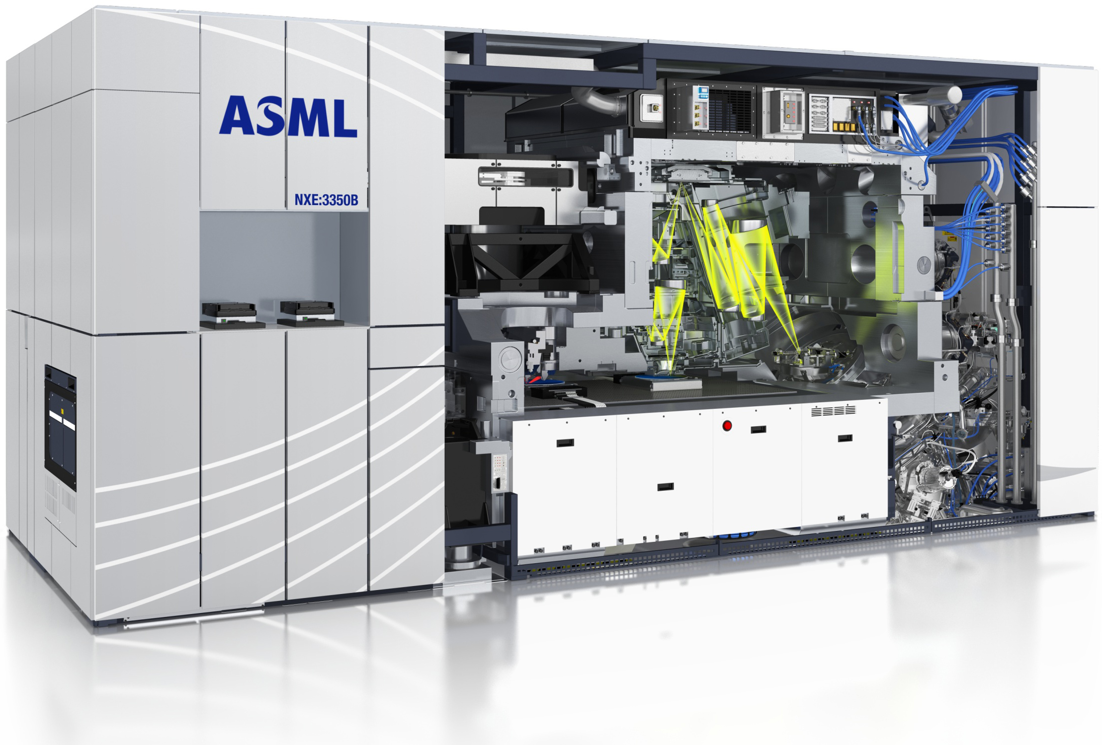
Since Samsung plans to start risk production using the 7LPP in the second half of 2018, the technology is hardly going to be used for high-volume manufacturing before the second half of 2019. Keeping in mind that Samsung now begins HVM using its leading-edge process technologies in October, it is possible that it is going to kick-off 7LPP HVM in fall 2019, but the 8LPP will be Samsung’s most advanced process technology for the better part of the year. Samsung does not mention timeframes for its 6 nm process technology and what to expect from it, but it is logical to assume that it will require more layers to be processed using ASML's EUV tools (like the NXE:3350B pictured above) in a bid to provide PPA advantages and it not be used for high-volume manufacturing before late 2020.
In March, Samsung only made brief announcements regarding its 10LPU, 8LPP and 6 nm process technology without disclosing their exact specifications or even PPA improvements targets. The addition of at least two more DUV technologies (the 10LPU and the 8LPP) in general may indicate that EUV may not be the best choice for all applications in 2019 – 2021, which is perfectly logical. Then again, we do not know how DUV and EUV technologies will co-exist early in the EUV era.
We are going to learn more about Samsung’s plans in the foundry industry in late May, when the company hosts its 2017 U.S Samsung Foundry Forum. So, we will have to wait for a couple of months for Samsung to disclose the whole picture regarding its upcoming process technologies.


89 Comments
View All Comments
melgross - Saturday, May 6, 2017 - link
A lot of chip experts don't believe that a true 5nm is possible. Not because we can't build it, but because the laws of physics are closing in. At that point, we have no substitute for FinFET, which doesn't work below 7 nm, and the three technologies that have been considered as a replacement aren't working either.When you begin to have features that are just 10 to 12 atoms wide, Heisenberg's Law hits you hard. As many electrons that travel through the feature, escape it. That's a death hell. So I expect that 7nm will really be 10 to 14 for most fabs, the way 14 is really 16 to 20 for most now.
The next step is expected to be carbon nanotubes, which both Hp and ibm have been working for years, and have shown limited success. That hoped to be ready, in limited complexity, by 2005 to 2030.
But there will be a wide gap between any silicon technology and that, even assuming they can get it working on a commercial basis at all. There are still too many steps for that, and they don't yet know how to climb them, or even if they're there.
melgross - Saturday, May 6, 2017 - link
Oops, too many typos. I meant, ready by 2025 to 2030, of course.Meteor2 - Sunday, May 7, 2017 - link
You're right, but I think between EUV and further development of the new gate concepts we'll make 5 nm happen. Although as really it's a question of whether commercial interests will fund the R&D, rather can 'science' make it happen, I suppose there's a risk 5 nm won't happen as designing such chips will be fantastically expensive. Will we be prepared to spend the $$$ for the performance which would be delivered?lefty2 - Friday, May 5, 2017 - link
Intel already has lost it's process advantage. Samsung's 10nm is currently in HVM and denser than Intel's 14nm. Intel say they will launch 10nm in 2017, but the yields are so bad they can hardly be considered production yield. By the time it reaches production yield TSMC will have 7nmDrumsticks - Friday, May 5, 2017 - link
Intel's 10nm is going to be denser than Samsung or TSMC's 7nm imo, going by the numbers we see here. Intel's 14nm is already denser than their competition by somewhere in the realm of 30% (per the hard numbers Intel released a few weeks back, and nobody has contradicted them). Intel's jump to 10nm is going to provide ~2.7x higher density than their 14nm node, and I think they've said several times they plan to ship 10nm this year.Even with a 70% area reduction on 7nm vs 16nm at TSMC, I don't think that overcomes a 30% lead + a 2.7x increase in density on top of that lead.
For another comparison, Intel's 10nm measures 100M transistors / mm^2, versus their competition at 50M / mm^2 at 10nm. Assuming TSMC's transistor density is around the "Others" metric, a 37% reduction in area from 10nm to 7nm would still leave them short of Intel's process node. I suspect everybody else will need a 5nm node to temporarily jump ahead of Intel's 10nm, before Intel's 7nm rolls around in 2020 or something and puts everybody behind again.
Numbers come from https://newsroom.intel.com/newsroom/wp-content/upl... which based on most of what I've seen has been accepted as a well done report. I'd love to see everybody switch to a more objective metric, since process node is now just a marketing game.
vladx - Friday, May 5, 2017 - link
They obviously can't compete with Intel head-to-head so say they have to resort to marketing gimmicks to make it appear they're coming ahead.SuperMecha - Saturday, May 6, 2017 - link
Intel's 14nm density advantage compared to GF/Samsung's 14nm process is only 23% not 30%. Also Intel's recent presentation only compares up to their competitor's 10nm not 7nm. In 2018 Intel will lose it transistor density advantage.https://www.semiwiki.com/forum/content/6713-14nm-1...
Drumsticks - Saturday, May 6, 2017 - link
I know Intel compared to the 10nm products; I was just extrapolating from that based on what TSMC stated (in the article) about their 7nm vs their own 16nm and 10nm. With everybody using different statistics now for each of their parts, it's not surprising that Intel gets passed every now and then, considering the time between their nodes is getting longer and longer.lefty2 - Saturday, May 6, 2017 - link
Scotten Jones did a detailed analysis of various leading edge nodes and concluded that TSMC's 7nm is slightly denser than Intel's 10nm and Samsun/TSMC 10nm is slightly desnser than Intel's 14nm:https://www.semiwiki.com/forum/content/6713-14nm-1...
Intel's 2017 launch of 10nm is virtually a paper launch. They are only going to release a couple of low volume SKUs at the very end of 2017, just so they can claim that they have the process lead. It's not till late 2018, or 2019 that the bulk of their products go to 10nm. Also the first iteration of 10nm performs worse than Intel's current 14nm+ process.
melgross - Saturday, May 6, 2017 - link
I don't believe it. First of all, neither he, or anyone else outside those companies actually knows enough about the actual chips to know the true density. Evaluating these by making some basic mathematical calculations doesn't tell us anything about the actual processes. It's all theoretical.