The Intel Optane SSD DC P4800X (375GB) Review: Testing 3D XPoint Performance
by Billy Tallis on April 20, 2017 12:00 PM EST3D XPoint Refresher
Intel's 3D XPoint memory technology is fundamentally very different from NAND flash. Intel has not clarified any more low-level details since their initial joint announcement with Micron of this technology, so our analysis from 2015 is still largely relevant. The industry consensus is that 3D XPoint is something along the lines of a phase change memory or conductive bridging resistive RAM, but we won't know for sure until third parties put 3D XPoint memory under an electron microscope.
Even without knowing the precise details, the high-level structure of 3D XPoint confers some significant advantages and disadvantages relative to NAND flash or DRAM. 3D XPoint can be read or written at the bit or word level, which greatly simplifies random access and wear leveling as compared to the multi-kB pages that NAND flash uses for read or program operations and the multi-MB blocks used for erase operations. Where DRAM requires a transistor for each memory cell, 3D XPoint isolates cells from each other by stacking them each in series with a diode-like selector. This frees up 3D XPoint to use a multi-layer structure, though not one that is as easy to manufacture as 3D NAND flash. This initial iteration of 3D XPoint uses just two layers and provides a per-die capacity of 128Gb, a step or two behind NAND flash but far ahead of the density of DRAM. 3D XPoint is currently storing just one bit per memory cell while today's NAND flash is mostly storing two or three bits per cell. Intel has indicated that the technology they are using, with sufficient R&D, can support more bits per cell to help raise density.
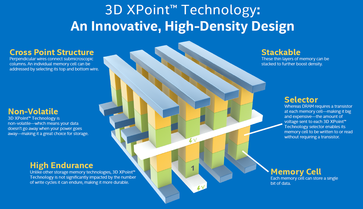
The general idea of a resistive memory cell paired with a selector and built at the intersections of word and bit lines is not unique to 3D XPoint memory. The term "crosspoint" has been used to describe several memory technologies with similar high-level architectures but different implementation details. As one Intel employee has explained, it is relatively easy to discover a material that exhibits hysteresis and thus has the potential to be used as a memory cell. The hard part is desiging a memory cell and selector that are fast, durable, and manufacturable at scale. The greatest value in Intel's 3D XPoint technology is not the high-level design but the specific materials and manufacturing methods that make it a practical invention. It has been noted by some analysts that the turning point for technologies such as 3D XPoint may very well be in the development in the selector itself, which is believed to be a Schottky diode or an ovonic selector.
In addition to the advantages that any resistive memory built on a crosspoint array can expect, Intel's 3D XPoint memory is supposed to offer substantially higher write endurance than NAND flash, and much lower read and write times. Intel has only quantified the low-level performance of 3D XPoint memory with rough order of magnitude comparisons against DRAM and NAND flash in general, so this test of the Optane SSD DC P4800X is the first chance to get some precise data. Unfortunately, we're only indirectly observing the capabilities of 3D XPoint, because the Optane SSD is still a PCIe SSD with a controller translating the block-oriented NVMe protocol and providing wear leveling.
The only other Optane product Intel has announced so far is another PCIe SSD, but on an entirely different scale: the Optane Memory product for consumers uses just one or two 3D XPoint chips and is intended to serve as a 32GB cache device accelerating access to a mechanical hard drive or slower SATA SSD. Next year Intel will start talking about putting 3D XPoint on DIMMs, and by then if not sooner we should have more low-level information about 3D XPoint technology.


117 Comments
View All Comments
ddriver - Friday, April 21, 2017 - link
*450 ns, by which I mean lower by 450 ns. And the current xpoint controller is nowhere near hitting the bottleneck of PCIE. It would take a controller that is at least 20 times faster than the current one to even get to the point where PCIE is a bottleneck. And even faster to see any tangible benefit from connecting xpoint directly to the memory controller.I'd rather have some nice 3D SLC (better than xpoint in literally every aspect) on PCIE for persistent storage RAM in the dimm slots. Hyped as superior, xpoint is actually nothing but a big compromise. Peak bandwidth is too low even compared to NVME NAND, latency is way too high and endurance is way too low for working memory. Low queue depths performance is good, but credit there goes to the controller, such a controller will hit even better performance with SLC nand. Smarter block management could also double the endurance advantage SLC already has over xpoint.
mdriftmeyer - Saturday, April 22, 2017 - link
ddriver is spot on. just to clarify an early comment. He's correct and the IntelUser2000 is out of his league.mdriftmeyer - Saturday, April 22, 2017 - link
Spot on.tuxRoller - Friday, April 21, 2017 - link
We don't know how much slower the media is than dram right now.We know than using dram over nvme has similar (though much better worst case) perf to this.
See my other post regarding polling and latency.
bcronce - Saturday, April 22, 2017 - link
Re-reading, I see it says "typical" latency is under 10us, placing it in spitting distance of DDR3/4. It's the 99.9999th percentile that is 60us for Q1. At Q16, 99.999th percentile is 140us. That means it takes only 140us to service 16 requests. That's pretty much the same as 10us.Read Q1 4KiB bandwidth is only about 500MiB/s, but at Q8, it's about 2GiB which puts it on par with DDR4-2400.
ddriver - Saturday, April 22, 2017 - link
"placing it in spitting distance of DDR3/4"I hope you do realize that dram latency is like 50 NANOseconds, and 1 MICROsecond is 1000 NANOseconds.
So 10 us is actually 200 times as much as 50 ns. Thus making hypetane about 200 times slower in access latency. Not 200%, 200X.
tuxRoller - Saturday, April 22, 2017 - link
Yes, the dram media is that fast but when it's exposed through nvme it has the latency characteristics that bcronce described.wumpus - Sunday, April 23, 2017 - link
That's only on a page hit. For the type of operations that 3dxpoint is looking at (4k or so) you won't find it on an open page and thus take 2-3 times as long till it is ready.That still leaves you with ~100x latency. And we are still wondering if losing the PCIe controller will make any significant difference to this number (one problem is that if Intel/Micron magically fixed this, the endurance is only slightly better than SLC and would quickly die if used as main memory).
ddriver - Sunday, April 23, 2017 - link
Endurance for the initial batch postulated from intel's warranty would be around 30k PE cycles, and 50k for the upcoming generation. That's not "only slightly better than SLC" as SCL has 100k PE cycles endurance. But the 100k figure is somewhat old, and endurance goes down with process node. So at a comparable process, SLC might be going down, approaching 50k.It remains to be seen, the lousy industry is penny pinching and producing artificial NAND shortages to milk people as much as possible, and pretty much all the wafers are going into TLC, some MLC and why oh why, QLC trash.
I guess they are saving the best for last. 3D SLC will address the lower density, samsung currently has 2 TB MLC M2, so 1 TB is perfectly doable via 3D SLC. I am guessing samsung's z-nand will be exactly that - SLC making a long overdue comeback.
tuxRoller - Sunday, April 23, 2017 - link
The endurance issue is, imho, the biggest concern right now.