The AMD Zen and Ryzen 7 Review: A Deep Dive on 1800X, 1700X and 1700
by Ian Cutress on March 2, 2017 9:00 AM ESTExecution, Load/Store, INT and FP Scheduling
The execution of micro-ops get filters into the Integer (INT) and Floating Point (FP) parts of the core, which each have different pipes and execution ports. First up is the Integer pipe which affords a 168-entry register file which forwards into four arithmetic logic units and two address generation units. This allows the core to schedule six micro-ops/cycle, and each execution port has its own 14-entry schedule queue.
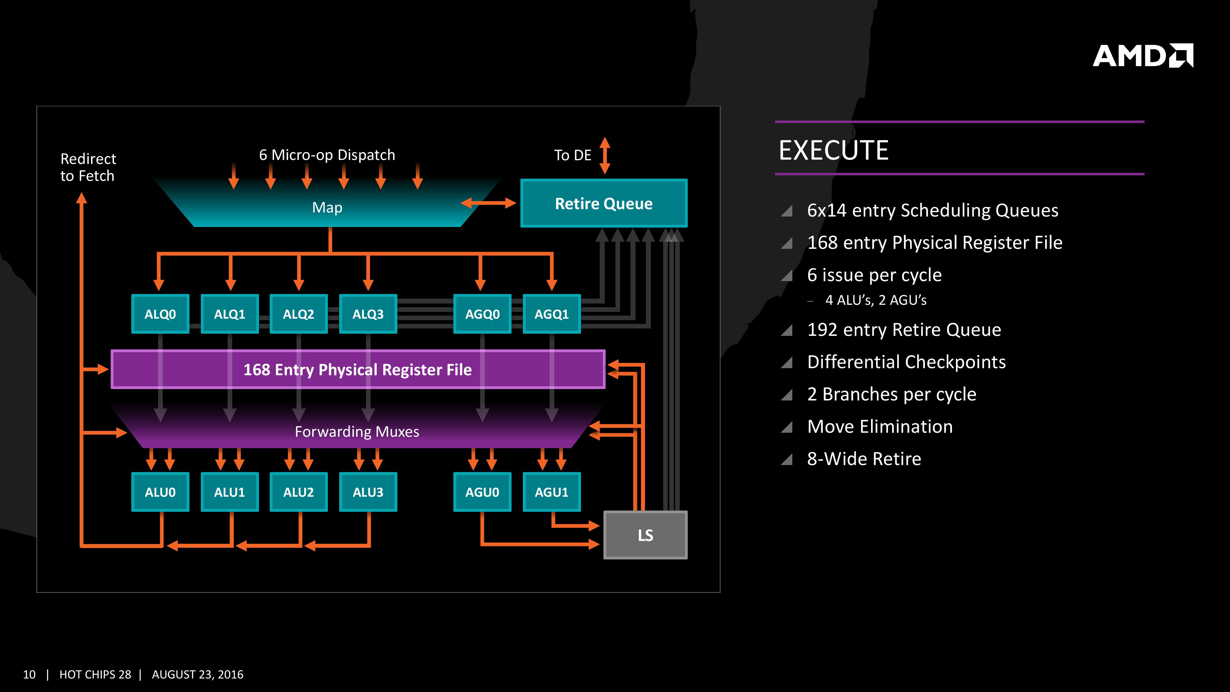
The INT unit can work on two branches per cycle, but it should be noted that not all the ALUs are equal. Only two ALUs are capable of branches, one of the ALUs can perform IMUL operations (signed multiply), and only one can do CRC operations. There are other limitations as well, but broadly we are told that the ALUs are symmetric except for a few focused operations. Exactly what operations will be disclosed closer to the launch date.
The INT pipe will keep track of branching instructions with differential checkpoints, to cut down on storing redundant data between branches (saves queue entries and power), but can also perform Move Elimination. This is where a simple mov command between two registers occurs – instead of inflicting a high energy loop around the core to physically move the single instruction, the core adjusts the pointers to the registers instead and essentially applies a new mapping table, which is a lower power operation.
Both INT and FP units have direct access to the retire queue, which is 192-entry and can retire 8 instructions per cycle. In some previous x86 CPU designs, the retire unit was a limiting factor for extracting peak performance, and so having it retire quicker than dispatch should keep the queue relatively empty and not near the limit.
The Load/Store Units are accessible from both AGUs simultaneously, and will support 72 out-of-order loads. Overall, as mentioned before, the core can perform two 16B loads (2x128-bit) and one 16B store per cycle, with the latter relying on a 44-entry Store queue. The TLB buffer for the L2 cache for already decoded addresses is two level here, with the L1 TLB supporting 64-entry at all page sizes and the L2 TLB going for 1.5K-entry with no 1G pages. The TLB and data pipes are split in this design, which relies on tags to determine if the data is in the cache or to start the data prefetch earlier in the pipeline.
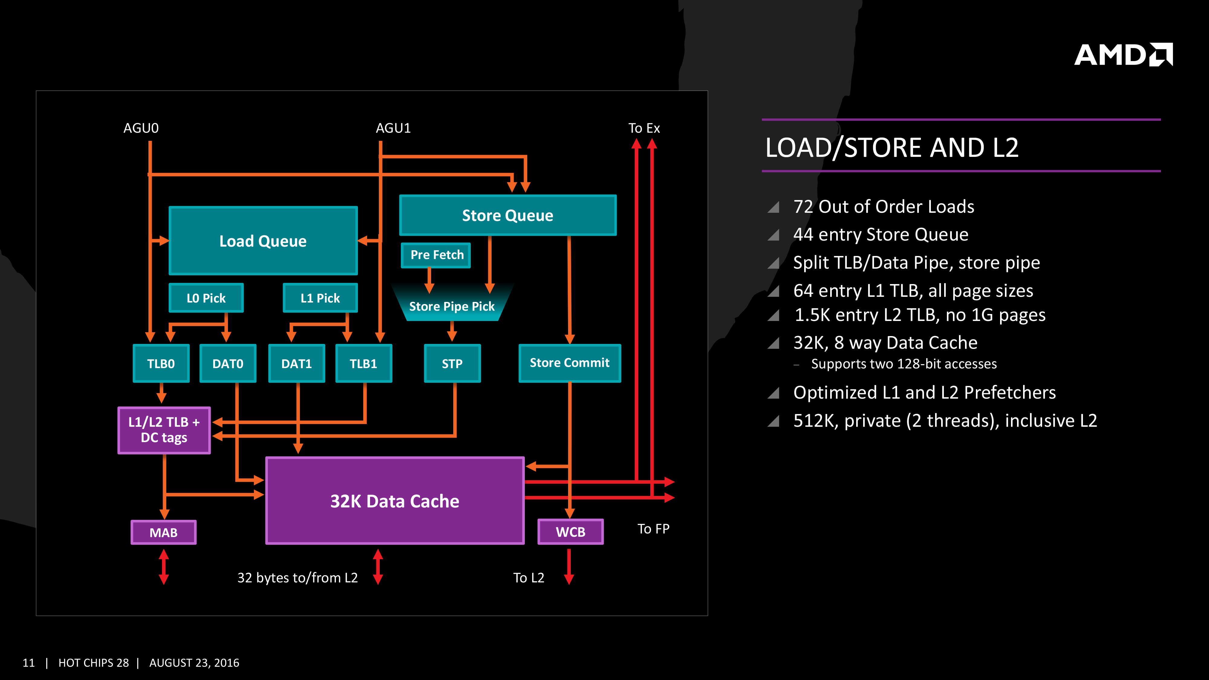
The data cache here also has direct access to the main L2 cache at 32 Bytes/cycle, with the 512 KB 8-way L2 cache being private to the core and inclusive. When data resides back in L1 it can be processed back to either the INT or the FP pipes as required.
Moving onto the floating point part of the core, and the first thing to notice is that there are two scheduling queues here. These are listed as ‘schedulable’ and ‘non-schedulable’ queues with lower power operation when certain micro-ops are in play, but also allows the backup queue to sort out parts of the dispatch in advance via the LDCVT. The register file is 160 entry, with direct FP to INT transfers as required, as well as supporting accelerated recovery on flushes (when data is written to a cache further back in the hierarchy to make room).
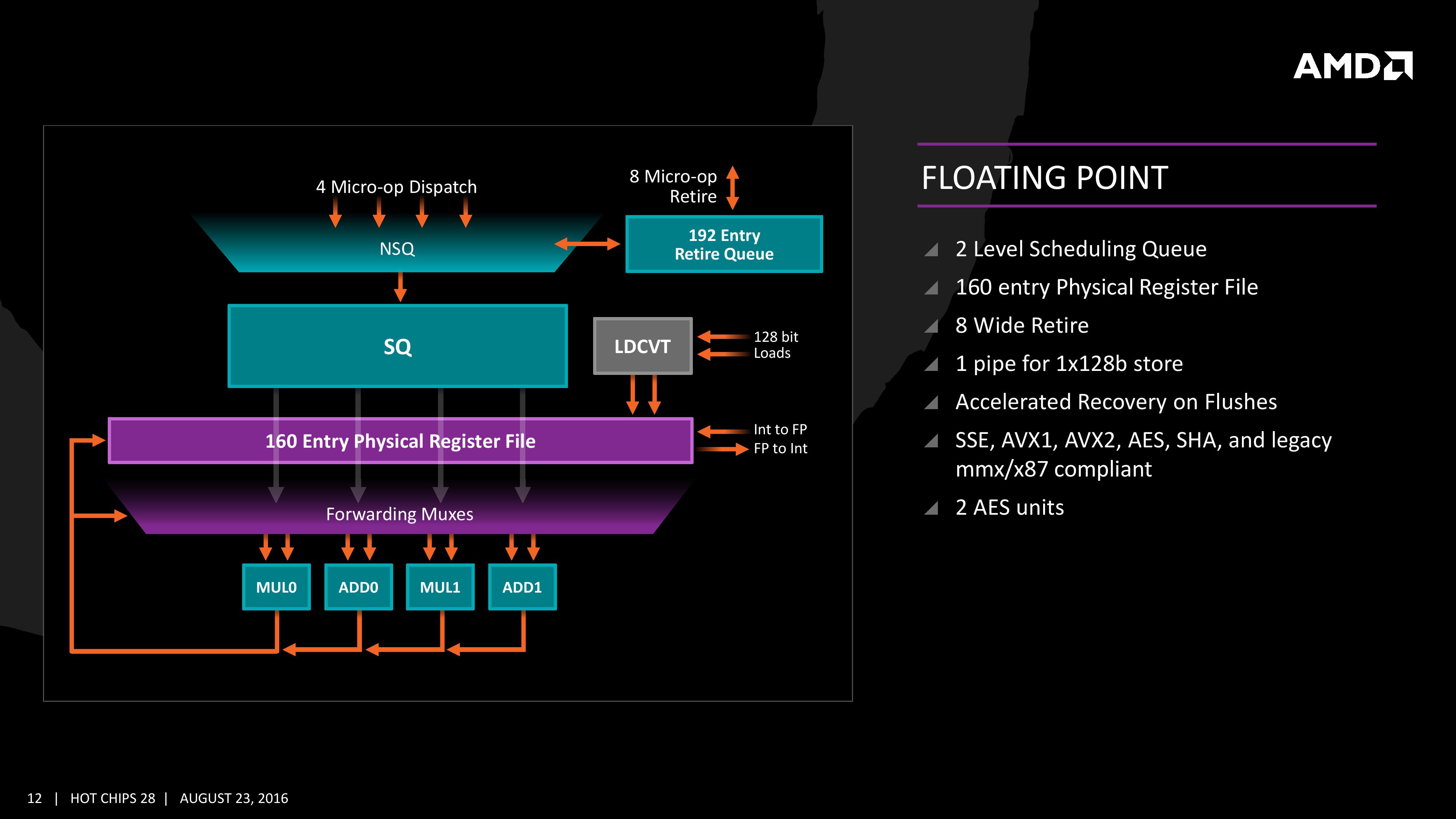
The FP Unit uses four pipes rather than three on Excavator, and we are told that the latency in Zen is reduced as well for operations (though more information on this will come at a later date). We have two MUL and two ADD in the FP unit, capable of joining to form two 128-bit FMACs, but not one 256-bit AVX. In order to do AVX, the unit will split the operations accordingly. On the counter side each core will have 2 AES units for cryptography as well as decode support for SSE, AVX1/2, SHA and legacy mmx/x87 compliant code.


574 Comments
View All Comments
nt300 - Saturday, March 11, 2017 - link
If AMD hadn't gone with GF's 14nm process, ZEN would probably have been delayed. I think as soon as Ryzen Optimizations come out, these chips will further outperform.MongGrel - Thursday, March 9, 2017 - link
For some reason making a casual comment about anything bad about the chip will get you banned at the drop of a hat on the tech forums, and then if you call him out they will ban you more.
https://arstechnica.com/gadgets/2017/03/amds-momen...
MongGrel - Thursday, March 9, 2017 - link
For some reason, MarkFW seems to thinks he is the reincarnation of Kyle Bennet, and whines a lot before retreating to his safe space.nt300 - Saturday, March 11, 2017 - link
I've noticed in the past that AMD has an issue with increasing L3 cache speed and/or Latencies. Hopefully they start tightening the L3 as much as possible. Can Anandtech do a comparison between Ryzen before Optimizations and after Optimizations. Tyalpha754293 - Friday, March 17, 2017 - link
Looks like that for a lot of the compute-intensive benchmarks, the new Ryzen isn't that much better than say a Core i5-7700K.That's quite a bit disappointing.
AMD needs to up their FLOPS/cycle game in order to be able to compete in that space.
Such a pity because the original Opterons were a great value proposition vs. the Intels. Now, it doesn't even come close.
deltaFx2 - Saturday, March 25, 2017 - link
@Ian Cutress: When you do test gaming, if you can, I'd love to have the hypothesis behind the 'generally accepted methodology' tested out. The methodology being, to test it at lowest resolution. The hypothesis is that this stresses the CPU, and that a future, higher performance GPU will be bottlenecked by the slower CPU. Sounds logical, but is it?Here's the thing: Typically, when given more computing resources, people scale up their problem to utilize those resources. In other words, if I give you a more powerful GPU, games will scale up their perf requirements to match it, by doing stuff that were not possible/practical in earlier GPUs. Today's games are far more 'realistic' and are played at much higher resolutions than say 5 years ago. In which case, the GPU is always the limiting factor no matter what (unless one insists on playing 5 year old games on the biggest, baddest GPU). And I fully expect that the games of today are built to max out current GPUs, so hardware lags software.
This has parallels with what happens in HPC: when you get more compute nodes for HPC problems, people scale up the complexity of their simulations rather than running the old, simplified simulations. Amdahl's law is still not a limiting factor for HPC, and we seem to be talking about Exascale machines now. Clearly, there's life in HPC beyond what a myopic view through the Amdahl law lens would indicate.
Just a thought :) Clearly, core count requirements have gone up over the last decade, but is it true that a 4c/8t sandy bridge paired up with Nvidia's latest and greatest is CPU-bottlenecked at likely resolutions?
wavelength - Friday, March 31, 2017 - link
I would love to see Anand test against AdoredTV's most recent findings on Ryzen https://www.youtube.com/watch?v=0tfTZjugDegLawJikal - Friday, April 21, 2017 - link
What I'm surprised to see missing... in virtually all reviews across the web... is any discussion (by a publication or its readers) on the AM4 platform's longevity and upgradability (in addition to its cost, which is readily discussed).Any Intel Platform - is almost guaranteed to not accommodate a new or significantly revised microarchitecture... beyond the mere "tick". In order to enjoy a "tock", one MUST purchase a new motherboard (if historical precedent is maintained).
AMD AM4 Platform - is almost guaranteed to, AT LEAST, accommodate Ryzen "II" and quite possibly Ryzen "III" processors. And, in such cases, only a new processor and BIOS update will be necessary to do so.
This is not an insignificant point of differentiation.
PeterCordes - Monday, June 5, 2017 - link
The uArch comparison table has some errors for the Intel columns. Dispatch/cycle: Skylake can read 6 uops per clock from the uop cache into the issue queue, but the issue stage itself is still only 4 uops wide. You've labelled Even running from the loop buffer (LSD), it can only sustain a throughput of 4 uops per clock, same 4-wide pipeline width it has been since Core2. (pre-Haswell it has to be a mix of ALU and some store or load to sustain that throughput without bottlenecking on the execution ports.) Skylake's improved decode and uop-cache bandwidth lets it refill the uop queue (IDQ) after bubbles in earlier stages, keeping the issue stage fed (since the back-end is often able to actually keep up).Ryzen is 6-wide, but I think I've read that it can only issue 6 uops per clock if some of them are from "double instructions". e.g. 256-bit AVX like VADDPS ymm0, ymm1, ymm2 that decodes to two separate 128-bit uops. Running code with only single-uop instructions, the Ryzen's front-end throughput is 5 uops per clock.
In Intel terminology, "dispatch" is when the scheduler (aka Reservation Station) sends uops to the execution units. The row you've labelled "dispatch / cycle" is clearly the throughput for issuing uops from the front-end into the out-of-order core, though. (Putting them into the ROB and Reservation Station). Some computer-architecture people call that "dispatch", but it's probably not a good idea in an x86 context. (Unless AMD uses that terminology; I'm mostly familiar with Intel).
----
You list the uop queue size at 128 for Skylake. This is bogus. It's always 64 per thread, with or without hyperthreading. Intel has alternated in SnB/IvB/HSW/SKL between this and letting one thread use both queues as a single big queue. HSW/BDW statically partition their 56-entry queue into two 28-entry halves when two threads are active, otherwise it's a 56-entry queue. (Not 64). Agner Fog's microarch pdf and Intel's optmization manual both confirm this (in Section 2.1.1 about Skylake's front-end improvements over previous generations).
Also, the 4-uop per clock issue width is 4 fused-domain uops, so I was able to construct a loop that runs 7 unfused-domain uops per clock (http://www.agner.org/optimize/blog/read.php?i=415#... with 2 micro-fused ALU+load, one micro-fused store, and a dec/branch. AMD doesn't talk about "unfused" uops because it doesn't use a unified scheduler, IIRC, so memory source operands always stay with the ALU uop.
Also, you mentioned it in the text, but the L1d change from write-through to write-back is worth a table row. IIRC, Bulldozer's L1d write-back has a small buffer or something to absorb repeated writes of the same lines, so it's not quite as bad as a classic write-through cache would be for L2 speed/power requirements, but Ryzen is still a big improvement.