The AMD Zen and Ryzen 7 Review: A Deep Dive on 1800X, 1700X and 1700
by Ian Cutress on March 2, 2017 9:00 AM ESTPower, Performance, and Pre-Fetch: AMD SenseMI
Part of the demos leading up to the launch involved a Handbrake video transcode: a multithreaded test, showing a near-identical completion time between a high-frequency Ryzen without turbo compared to an i7-6900K at similar frequencies. Similarly we saw a Blender test we saw back in August achieving the same feat. AMD at the time also fired up some power meters, showing that Ryzen power consumption in that test was a few watts lower than the Intel part, implying that AMD is meeting its targets for power, performance and as a result, efficiency. The 52% improvement in IPC/efficiency is a result AMD seems confident that this target has been surpassed.

Leading up to the launch, AMD explained during our briefings that during the Zen design stages, up to 300 engineers were working on the core engine with an aggressive mantra of higher IPC for no power gain. This has apparently lead to over two million work hours of time dedicated to Zen. This is not an uncommon strategy for core designs. Part of this time will be spent devoping new power modes, and part of Zen is is that optimization and extension of the power/frequency curve: a key point in AMD’s new 5-stage ‘SenseMI’ technology.
SenseMI Stage 1: Pure Power
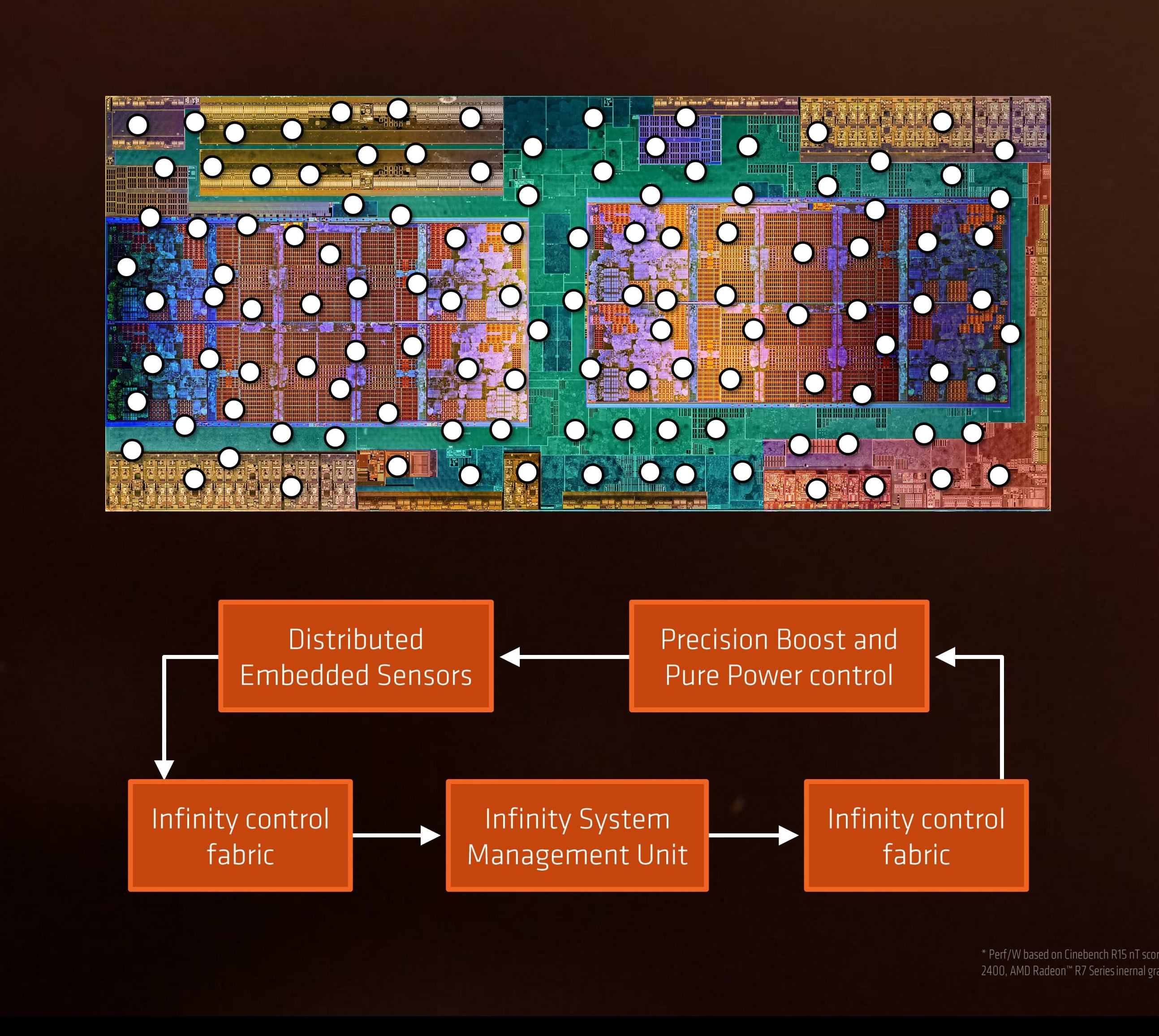
A number of recent microprocessor launches have revolved around silicon-optimized power profiles. We are now removed from the ‘one DVFS curve fits all’ application for high-end silicon, and AMD’s solution in Ryzen will be called Pure Power. The short explanation is that using distributed embedded sensors in the design (first introduced in bulk with Carrizo) that monitor temperature, speed and voltage, and the control center can manage the power consumption in real time. The glue behind this technology comes in form of AMD’s new ‘Infinity Fabric’.
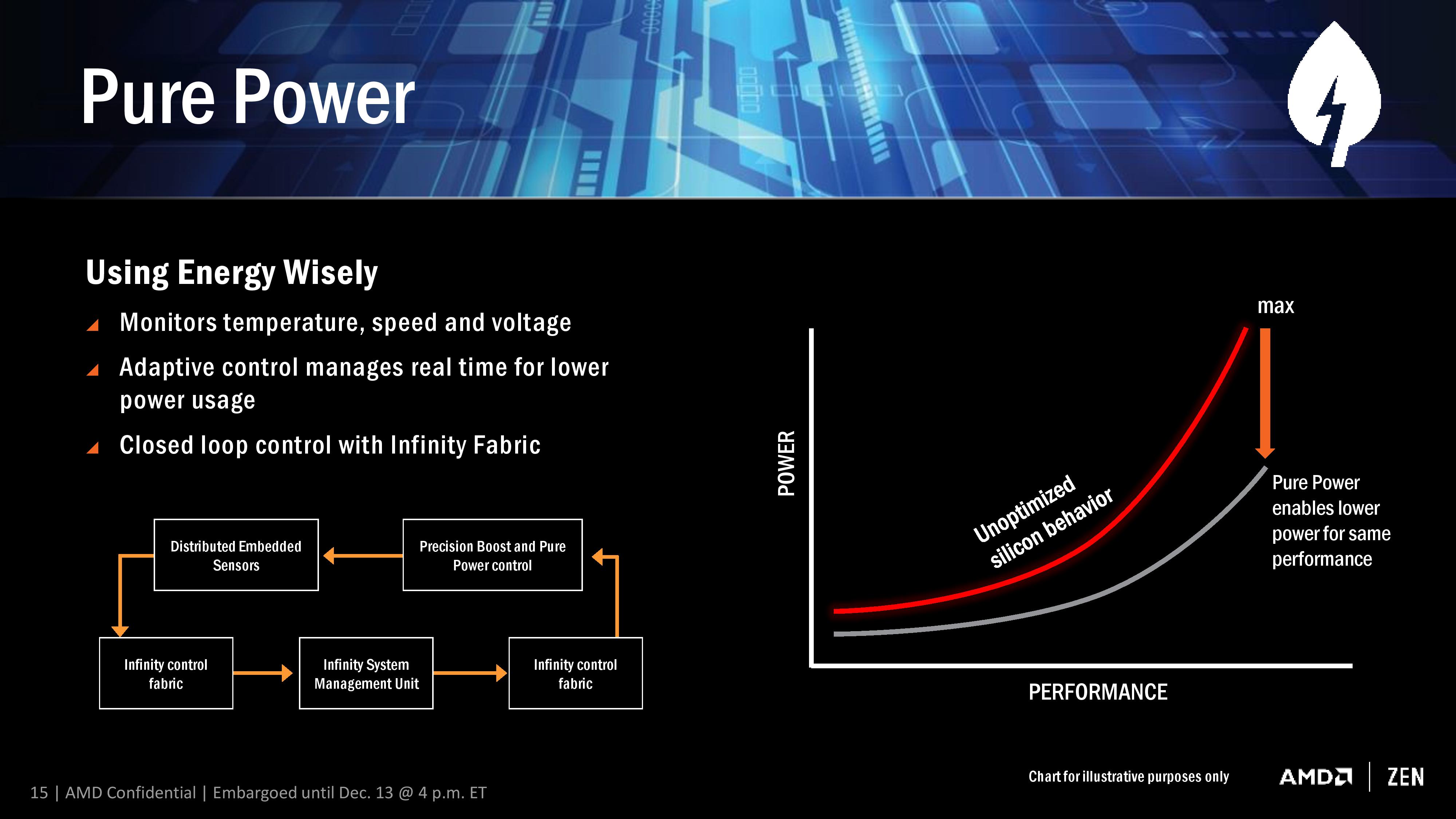
The fact that it’s described as a fabric means that it goes through the entire processor, connecting various parts together as part of that control. This is something wildly different to what we saw in Carrizo, aside from being the next-gen power adjustment and under a new name, and will permiate through Zen, Vega, and future AMD products.
The upshot of Pure Power is that the DVFS curve is lower and more optimized for a given piece of silicon than a generic DVFS curve, which results in giving lower power at various/all levels of performance. This in turn benefits the next part of SenseMI, Precision Boost.
SenseMi Stage 2: Precision Boost
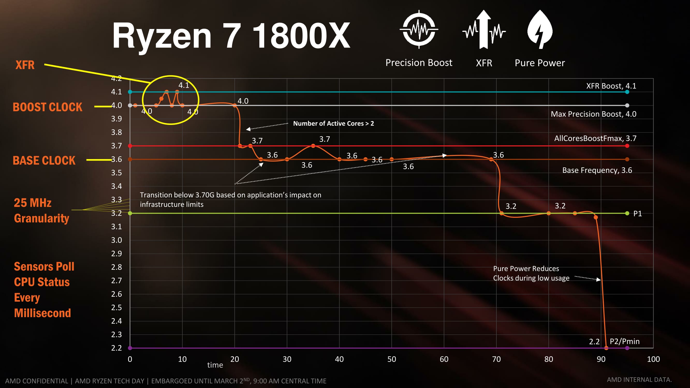
For almost a decade now, most commercial PC processors have invoked some form of boost technology to enable processors to use less power when idle and fully take advantage of the power budget when only a few elements of the core design is needed. We see processors that sit at 2.2 GHz that boost to 2.7 GHz when only one thread is needed, for example, because the whole chip still remains under the power limit. AMD is implementing Precision Boost for Ryzen, increasing the DVFS curve to better performance due to Pure Power, but also offering frequency jumps in 25 MHz steps which is new.
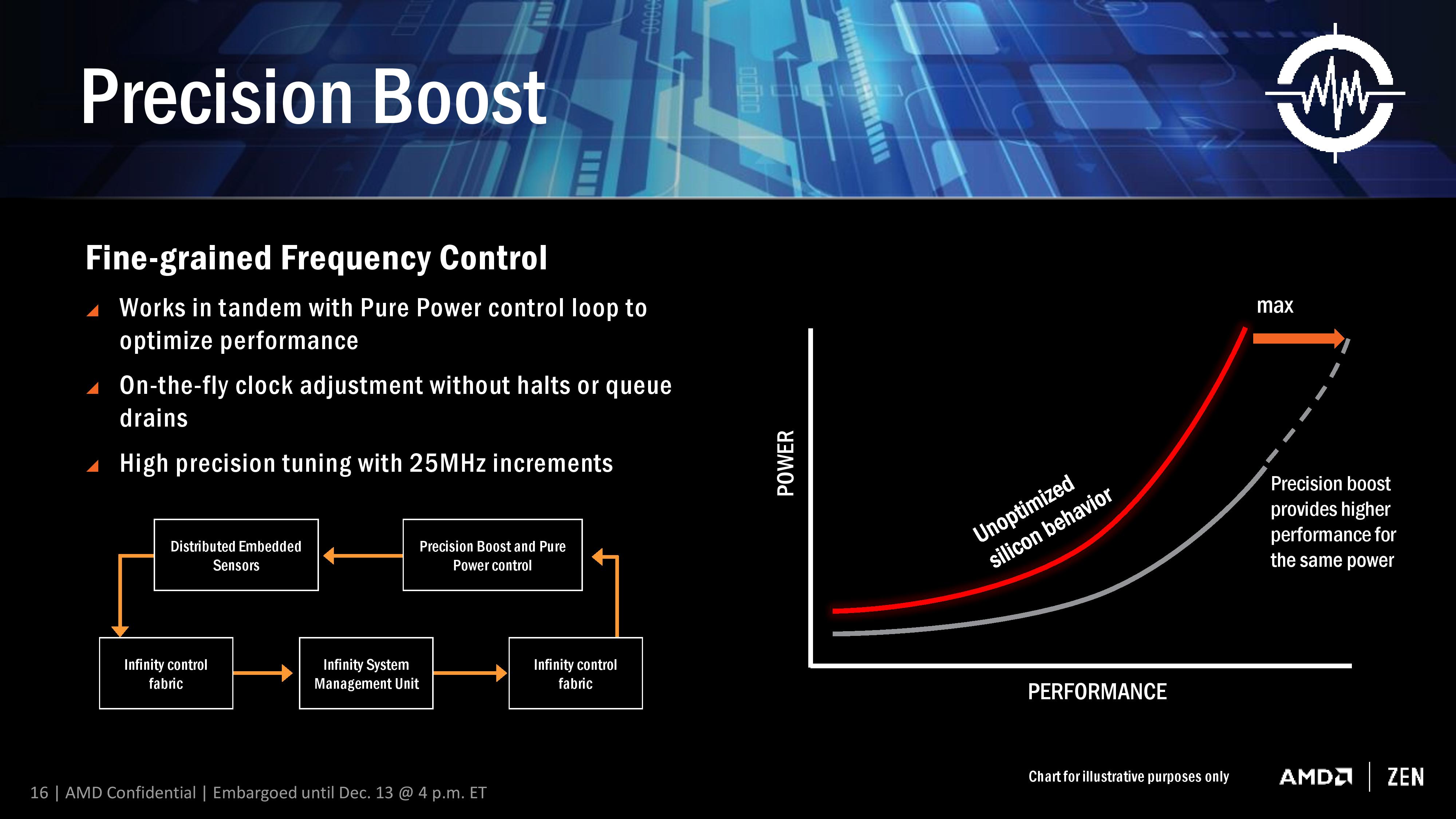
Precision Boost relies on the same Infinity Control Fabric that Pure Power does, but allows for adjustments of core frequency based on performance requirements and suitability/power given the rest of the core. The fact that it offers 25 MHz steps is surprising, however.
Current turbo control systems, on both AMD and Intel, are invoked by adjusting the CPU frequency multiplier. With the 100 MHz base clock on all modern CPUs, one step in frequency multiplier gives 100 MHz jump for the turbo modes, and any multiple of the multiplier can be used on the basis of whole numbers only.
With AMD moving to 25 MHz jumps in their turbo, this means either AMD can implement 0.25x fractional multipliers, similar to how processors in the early 2000s were able to negotiate 0.5x multiplier jumps. What this means in reality is that the processor has over 100 different frequencies it can potentially operate at, although control of the fractional multipliers below P0 is left to XFR (below).
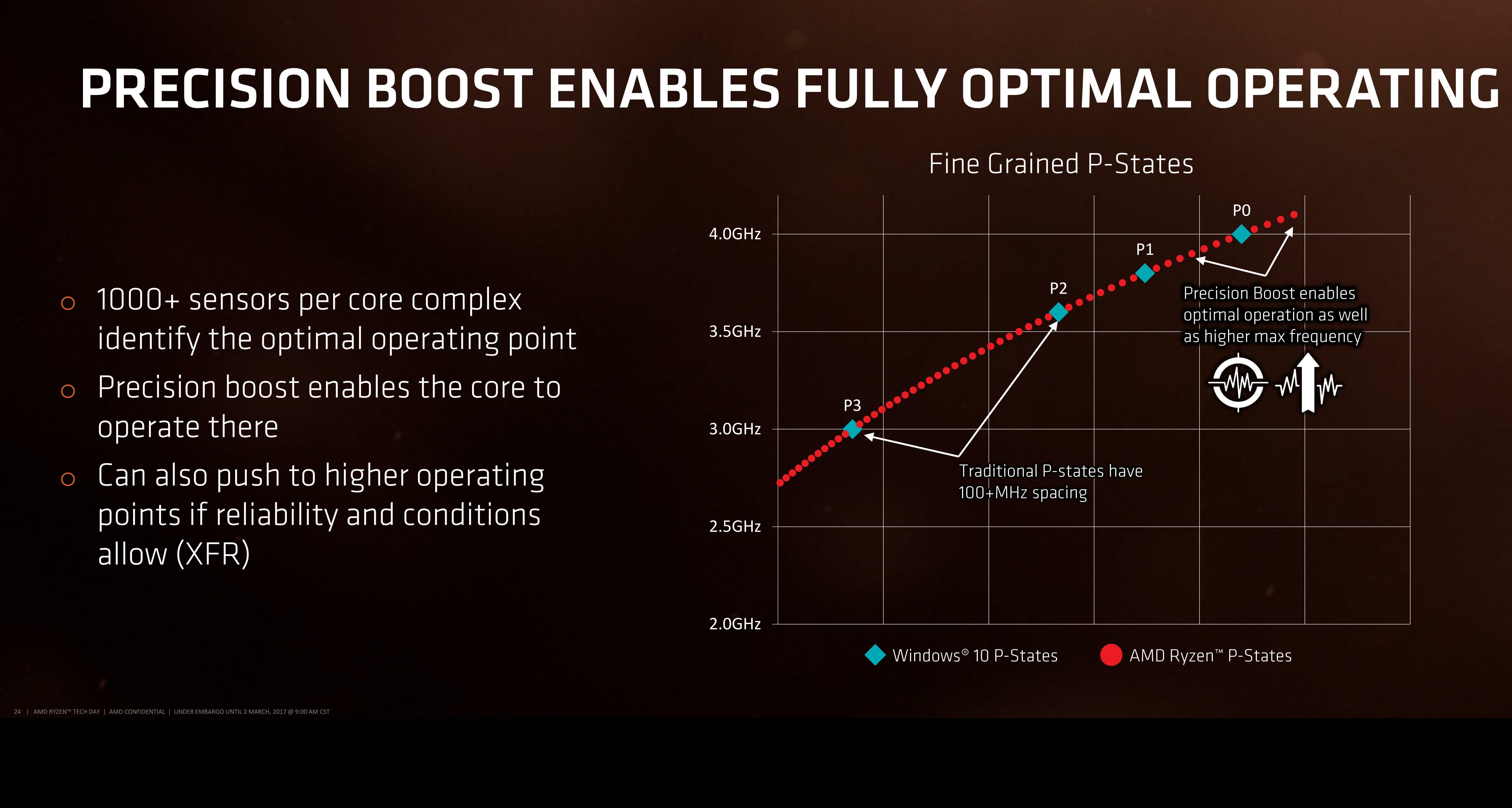
Part of this comes down to the extensive sensor technology, originally debuted for AMD in Carrizo at scale, but now offering almost 1000 sensors per chip to analyze at what frequency the core can run at. AMD controls all frequency of each core independently, which suggests that users might be able to find the highest performing core and lock important software on it.
If we consider that Zen’s original chief designer was Jim Keller (and his team), known for a number of older generation of AMD processors, a similar fractional multiplier technology might be in play here. If/when we get more information on it, we will let you know.
SenseMi Stage 3: Extended Frequency Range (XFR)
The main marketing points of on-the-fly frequency adjustment are typically down to low idle power and higher performance when needed. The current processors on the market have rated speeds on the box which are fixed frequency settings that can be chosen by the processor/OS depending on what level of performance is possible/required. AMD’s new XFR mode seems to do away with this, offering what sounds like an unlimited bound on performance.
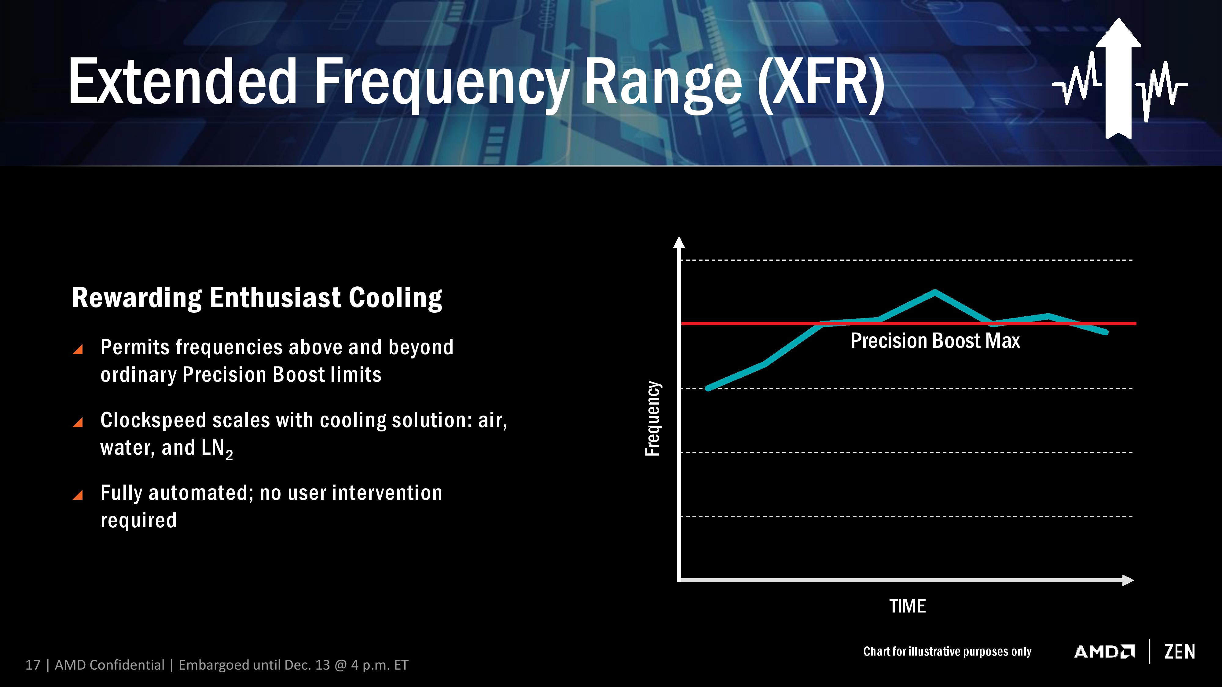
The concept here is that, beyond the rated turbo mode, if there is sufficient cooling then the CPU will continue to increase the clock speed and voltage until a cooling limit is reached. This is somewhat murky territory, though AMD claims that a multitude of different environments can be catered for the feature. AMD was not clear if this limit is determined by power consumption, temperature, or if they can protect from issues such as a bad frequency/voltage setting.
This is a dynamic adjustment rather than just another embedded look-up table such as P-states. AMD states that XFR is a fully automated system with no user intervention, although I suspect in time we might see an on/off switch in the BIOS. It also somewhat negates overclocking if your cooling can support it, which then brings up the issue for overclocking in general: casual users may not ever need to step into the overclocking world if the CPU does it all automatically.
I imagine that a manual overclock will still be king, especially for extreme overclockers competing with liquid nitrogen, as being able to personally fine tune a system might be better than letting the system do it itself. It can especially be true in those circumstances, as sensors on hardware can fail, report the wrong temperature, or may only be calibrated within a certain range.
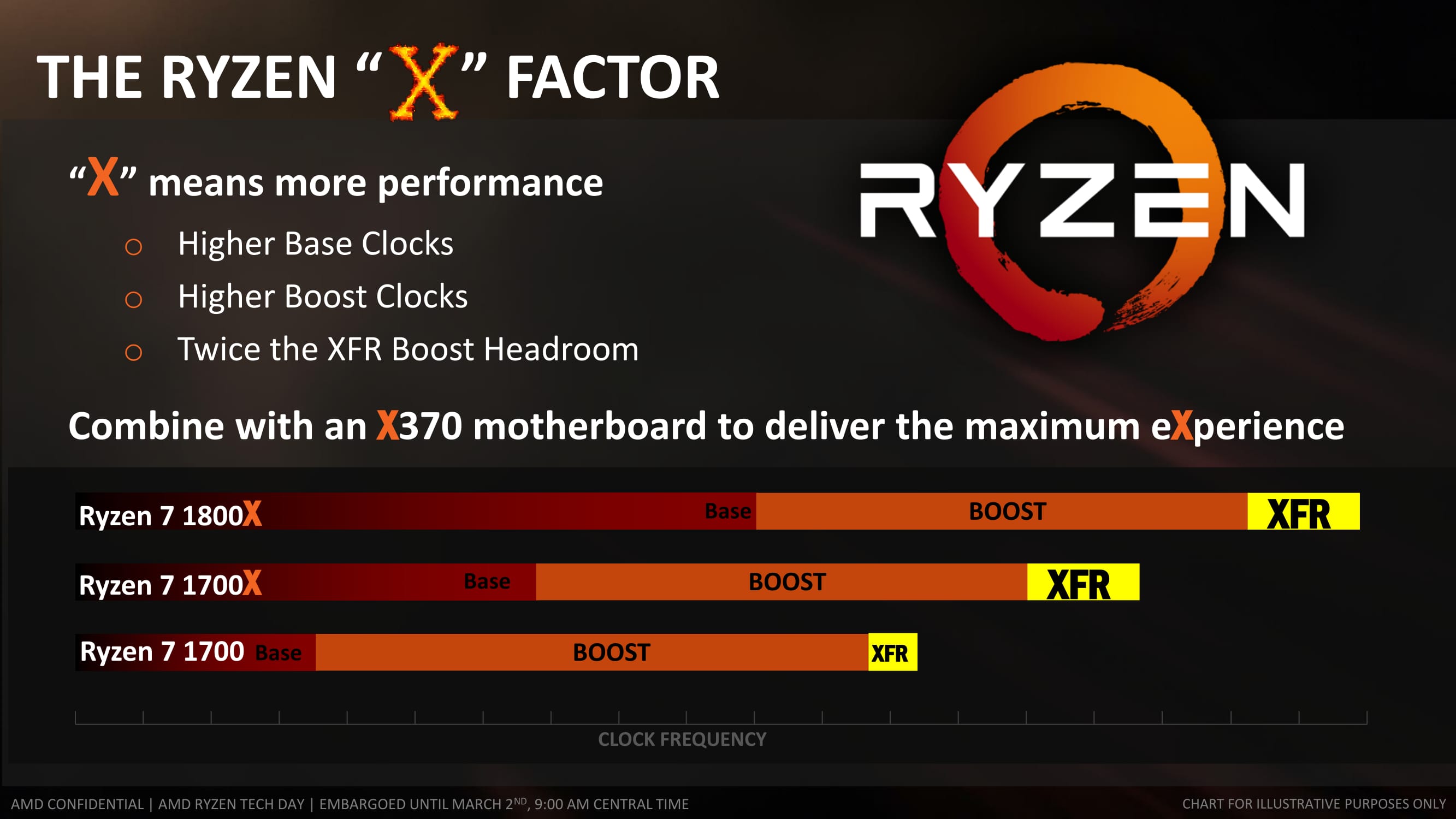
XFR will be on every consumer CPU (as the Zen microarchitecture is destined for server and mobile as well, XFR might have different connotations for both of those markets), and typically will allow for +100 MHz. CPUs that have the extra 'X' should allow for up to +200 MHz through XFR. This level of XFR is not set in stone, and may change in future CPUs.
SenseMi Stage 4+5: Neural Net Prediction and Smart Prefetch
Every generation of CPUs from the big companies come with promises of better prediction and better pre-fetch models. These are both important to hide latency within a core which might be created by instruction decode, queuing, or more usually, moving data between caches and main memory to be ready for the instructions. With Ryzen, AMD is introducing its new Neural Net Prediction hardware model along with Smart Pre-Fetch.
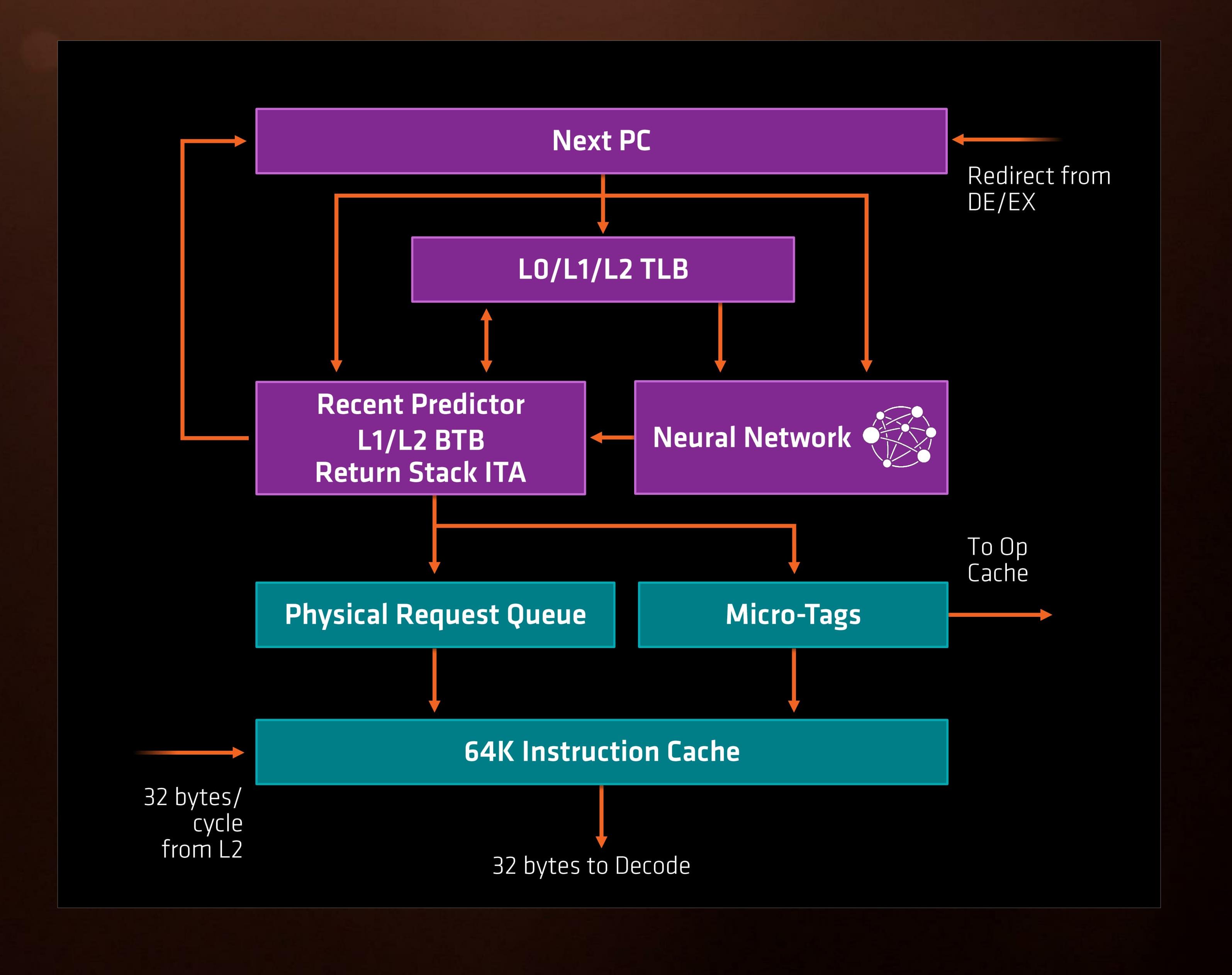
AMD is announcing this as a ‘true artificial network inside every Zen processor that builds a model of decisions based on software execution’. This can mean one of several things, ranging from actual physical modelling of instruction workflow to identify critical paths to be accelerated (unlikely) or statistical analysis of what is coming through the engine and attempting to work during downtime that might accelerate future instructions (such as inserting an instruction to decode into an idle decoder in preparation for when it actually comes through, therefore ends up using the micro-op cache and making it quicker).
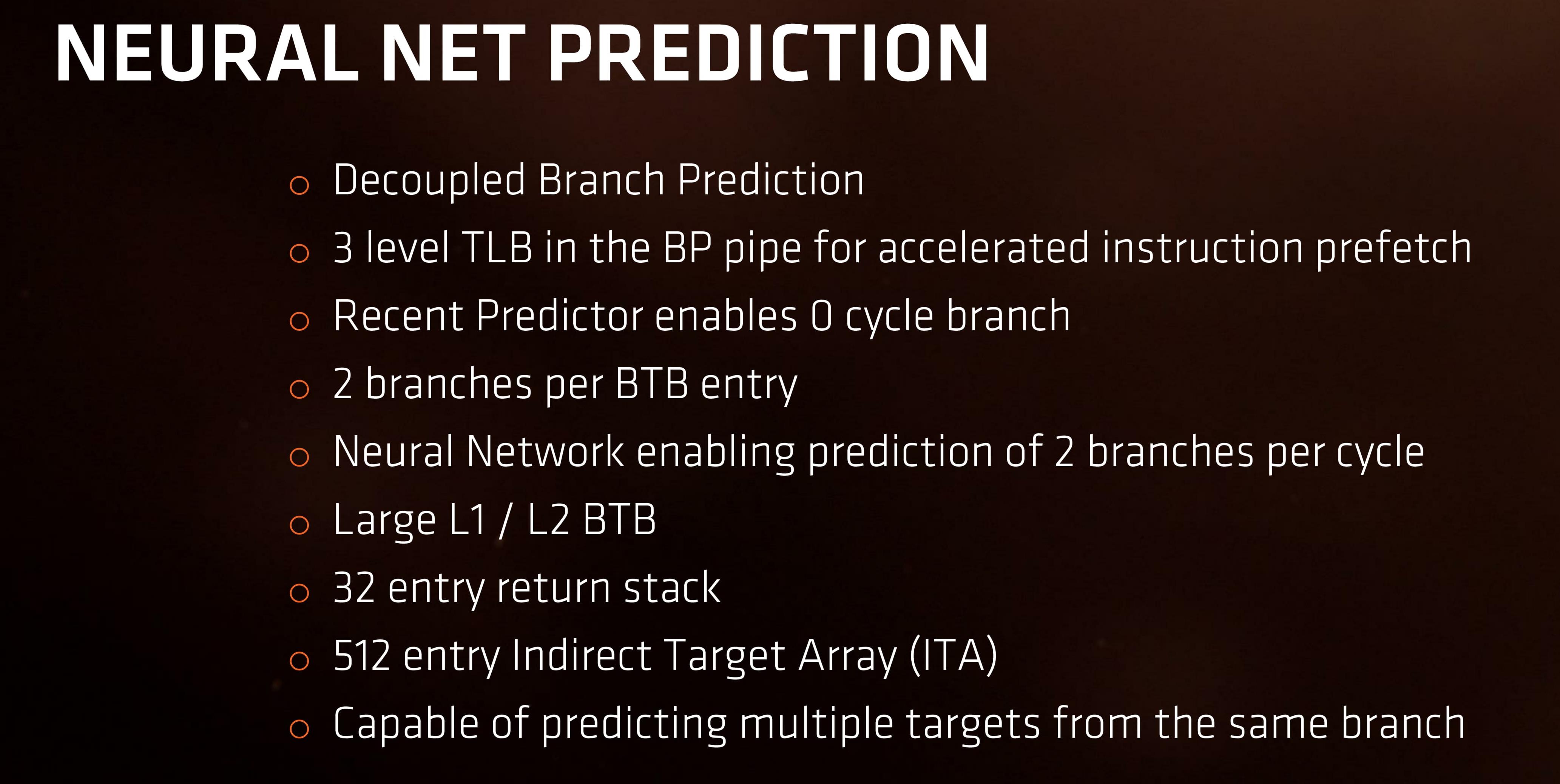
For Zen this means two branches can be predicted per cycle (so, one per thread per cycle), and a multi-level TLB to assist recently required instructions again. With these caches and buffers, typically doubling in size gets a hit rate of sqrt(2), or +41%, for double the die area, and it becomes a balance of how good you want it to be compared with how much floor plan area can be dedicated to it.
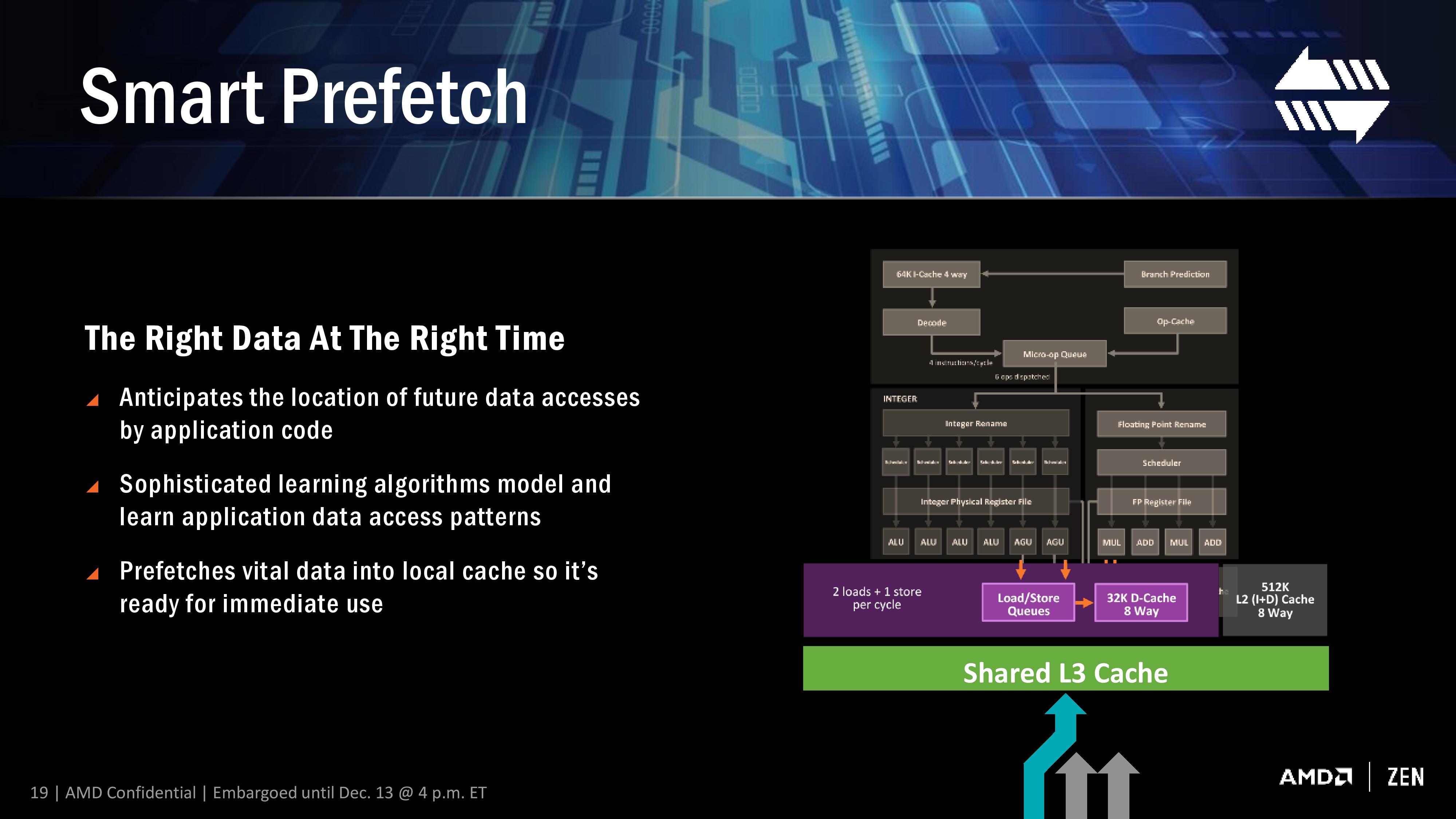
Modern processors already do decent jobs when repetitive work is being used, such as identifying when every 4th element in a memory array is being accessed, and can pull that data in earlier to be ready in case it is used. The danger of smart predictors however is being overly aggressive – pulling in too much data that old data might be ditched because it’s never used (over prediction), pulling in too much data such that it’s already evicted by the time the data is needed (aggressive prediction), or simply wasting excess power with bad predictions (stupid prediction…).
AMD is stating that Zen implements algorithm learning models for both instruction prediction and prefetch, which will no doubt be interesting to see if they have found the right balance of prefetch aggression and extra work in prediction.
It is worth noting here that AMD will likely draw upon the increased L3 bandwidth in the new core as a key element to assisting the prefetch, especially as the shared L3 cache is an exclusive victim cache and designed to contain data already used/evicted to be used again at a later date.


574 Comments
View All Comments
nt300 - Saturday, March 11, 2017 - link
If AMD hadn't gone with GF's 14nm process, ZEN would probably have been delayed. I think as soon as Ryzen Optimizations come out, these chips will further outperform.MongGrel - Thursday, March 9, 2017 - link
For some reason making a casual comment about anything bad about the chip will get you banned at the drop of a hat on the tech forums, and then if you call him out they will ban you more.
https://arstechnica.com/gadgets/2017/03/amds-momen...
MongGrel - Thursday, March 9, 2017 - link
For some reason, MarkFW seems to thinks he is the reincarnation of Kyle Bennet, and whines a lot before retreating to his safe space.nt300 - Saturday, March 11, 2017 - link
I've noticed in the past that AMD has an issue with increasing L3 cache speed and/or Latencies. Hopefully they start tightening the L3 as much as possible. Can Anandtech do a comparison between Ryzen before Optimizations and after Optimizations. Tyalpha754293 - Friday, March 17, 2017 - link
Looks like that for a lot of the compute-intensive benchmarks, the new Ryzen isn't that much better than say a Core i5-7700K.That's quite a bit disappointing.
AMD needs to up their FLOPS/cycle game in order to be able to compete in that space.
Such a pity because the original Opterons were a great value proposition vs. the Intels. Now, it doesn't even come close.
deltaFx2 - Saturday, March 25, 2017 - link
@Ian Cutress: When you do test gaming, if you can, I'd love to have the hypothesis behind the 'generally accepted methodology' tested out. The methodology being, to test it at lowest resolution. The hypothesis is that this stresses the CPU, and that a future, higher performance GPU will be bottlenecked by the slower CPU. Sounds logical, but is it?Here's the thing: Typically, when given more computing resources, people scale up their problem to utilize those resources. In other words, if I give you a more powerful GPU, games will scale up their perf requirements to match it, by doing stuff that were not possible/practical in earlier GPUs. Today's games are far more 'realistic' and are played at much higher resolutions than say 5 years ago. In which case, the GPU is always the limiting factor no matter what (unless one insists on playing 5 year old games on the biggest, baddest GPU). And I fully expect that the games of today are built to max out current GPUs, so hardware lags software.
This has parallels with what happens in HPC: when you get more compute nodes for HPC problems, people scale up the complexity of their simulations rather than running the old, simplified simulations. Amdahl's law is still not a limiting factor for HPC, and we seem to be talking about Exascale machines now. Clearly, there's life in HPC beyond what a myopic view through the Amdahl law lens would indicate.
Just a thought :) Clearly, core count requirements have gone up over the last decade, but is it true that a 4c/8t sandy bridge paired up with Nvidia's latest and greatest is CPU-bottlenecked at likely resolutions?
wavelength - Friday, March 31, 2017 - link
I would love to see Anand test against AdoredTV's most recent findings on Ryzen https://www.youtube.com/watch?v=0tfTZjugDegLawJikal - Friday, April 21, 2017 - link
What I'm surprised to see missing... in virtually all reviews across the web... is any discussion (by a publication or its readers) on the AM4 platform's longevity and upgradability (in addition to its cost, which is readily discussed).Any Intel Platform - is almost guaranteed to not accommodate a new or significantly revised microarchitecture... beyond the mere "tick". In order to enjoy a "tock", one MUST purchase a new motherboard (if historical precedent is maintained).
AMD AM4 Platform - is almost guaranteed to, AT LEAST, accommodate Ryzen "II" and quite possibly Ryzen "III" processors. And, in such cases, only a new processor and BIOS update will be necessary to do so.
This is not an insignificant point of differentiation.
PeterCordes - Monday, June 5, 2017 - link
The uArch comparison table has some errors for the Intel columns. Dispatch/cycle: Skylake can read 6 uops per clock from the uop cache into the issue queue, but the issue stage itself is still only 4 uops wide. You've labelled Even running from the loop buffer (LSD), it can only sustain a throughput of 4 uops per clock, same 4-wide pipeline width it has been since Core2. (pre-Haswell it has to be a mix of ALU and some store or load to sustain that throughput without bottlenecking on the execution ports.) Skylake's improved decode and uop-cache bandwidth lets it refill the uop queue (IDQ) after bubbles in earlier stages, keeping the issue stage fed (since the back-end is often able to actually keep up).Ryzen is 6-wide, but I think I've read that it can only issue 6 uops per clock if some of them are from "double instructions". e.g. 256-bit AVX like VADDPS ymm0, ymm1, ymm2 that decodes to two separate 128-bit uops. Running code with only single-uop instructions, the Ryzen's front-end throughput is 5 uops per clock.
In Intel terminology, "dispatch" is when the scheduler (aka Reservation Station) sends uops to the execution units. The row you've labelled "dispatch / cycle" is clearly the throughput for issuing uops from the front-end into the out-of-order core, though. (Putting them into the ROB and Reservation Station). Some computer-architecture people call that "dispatch", but it's probably not a good idea in an x86 context. (Unless AMD uses that terminology; I'm mostly familiar with Intel).
----
You list the uop queue size at 128 for Skylake. This is bogus. It's always 64 per thread, with or without hyperthreading. Intel has alternated in SnB/IvB/HSW/SKL between this and letting one thread use both queues as a single big queue. HSW/BDW statically partition their 56-entry queue into two 28-entry halves when two threads are active, otherwise it's a 56-entry queue. (Not 64). Agner Fog's microarch pdf and Intel's optmization manual both confirm this (in Section 2.1.1 about Skylake's front-end improvements over previous generations).
Also, the 4-uop per clock issue width is 4 fused-domain uops, so I was able to construct a loop that runs 7 unfused-domain uops per clock (http://www.agner.org/optimize/blog/read.php?i=415#... with 2 micro-fused ALU+load, one micro-fused store, and a dec/branch. AMD doesn't talk about "unfused" uops because it doesn't use a unified scheduler, IIRC, so memory source operands always stay with the ALU uop.
Also, you mentioned it in the text, but the L1d change from write-through to write-back is worth a table row. IIRC, Bulldozer's L1d write-back has a small buffer or something to absorb repeated writes of the same lines, so it's not quite as bad as a classic write-through cache would be for L2 speed/power requirements, but Ryzen is still a big improvement.