Intel Confirms 8th Gen Core on 14nm, Data Center First to New Nodes
by Ian Cutress on February 9, 2017 6:52 PM EST- Posted in
- CPUs
- Intel
- Core 8th Gen
- Cannon Lake
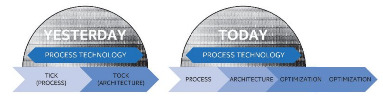
A quick news piece on information coming out of Intel’s annual Investor Day in California. As confirmed to Ashraf Eassa by Intel at the event, Intel’s 8th Generation Core microarchitecture will remain on the 14nm node. This is an interesting development with the recent launch of Intel’s 7th Generation Core products being touted as the ‘optimization’ behind the new ‘Process-Architecture-Optimization’ three-stage cadence that had replaced the old ‘tick-tock’ cadence. With Intel stringing out 14nm (or at least, an improved variant of 14nm as we’ve seen on 7th Gen) for another generation, it makes us wonder where exactly Intel can promise future performance or efficiency gains on the design unless they start implementing microarchitecture changes.
Despite this, if you were to believe supposed ‘leaked’ roadmaps (which we haven’t confirmed from a second source as of yet), the 8th Generation product ‘Cannon Lake’ is more geared towards the Y and U part of Intel’s roadmap. This would ring true with a mobile first strategy that Intel has mirrored with recent generations such that the smaller, low power chips are off the production line for a new product first, however we'd also expect 10nm to also be in the smaller chips first too (as demonstrated at CES). Where Cannon Lake will end up in the desktop or enterprise segment however remains to be seen. To put something a bit more solid into this, Ashraf also mentioned words from Dr. Venkata ‘Murthy’ Renduchintala, VP and GM of Client and IoT:
‘Murthy referred to it at the event, process tech use will be ‘fluid’ based on segment’.
If one read too much into this, we may start seeing a blend of process nodes for different segments at the same time for different areas of the market. We already do have that to some extent with the mainstream CPUs and the HEDT/Xeon families, but this phrasing seems that we might get another split between consumer products or consumer and enterprise. We may get to a point where Intel's 'Gen' naming scheme for its CPUs covers two or more process node variants.
Speaking of the Enterprise segment, another bit of information has also surfaced, coming from a slide during a talk by Diane Bryant (EVP/GM of Data Center) and posted online by Ashraf. The slide contains the words ‘Data center first for next process node’

We can either talk about process node in terms of the ‘number’, either 14nm/10nm/7nm, or by variants within that process (high power, high efficiency). One might suspect that this means Intel is moving hard and fast with 10nm for Xeons and big computing projects, despite showing off 10nm silicon at CES earlier this year. That being said, it’s important to remember that the data center market is large, and includes high-density systems with many cores, such as Atom cores, and Intel did recently open up its 10nm foundry business to ARM Artisan IP projects. So while the slide does say ‘Data center first’, it might be referring to DC projects based on ARM IP in that segment rather than big 4-24+ core Xeons. At this stage of the game it is hard to tell.
On top of all this, Intel still has extreme confidence in its foundry business. An image posted by Dick James of Siliconics from the livestream shows Intel expects to have a three-year process node advantage when its competitors (Samsung, TSMC) start launching 10nm:

I’ve been brief with this news for a reason - at this point there are a lot of balls in the air with many different ways to take this information, and the Investor Day is winding down on talks and finishing with smaller 1-on-1 meetings. We may get further clarification on this news as the day goes on.
Update 1: On speaking with Diane Bryant, the 'data center gets new nodes first' is going to be achieved by using multiple small dies on a single package. But rather than use a multi-chip package as in previous multi-core products, Intel will be using EMIB as demonstrated at ISSCC: an MCP/2.5D interposer-like design with an Embedded Multi-Die Interconnect Bridge (EMIB).
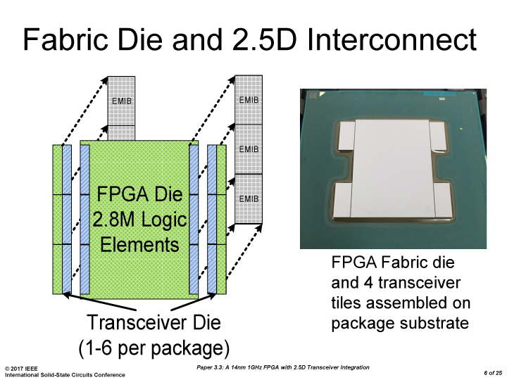
An Intel Slide from ISSCC, via PC Watch
Initially EMIB was thought of as a technology relating to Intel's acquisition of Altera and potential future embedded FPGA designs, and given the slide above and comments made at the Investor Day, it seems there are other plans for this technology too. The benefit of using multiple smaller dies over a large monolithic 600mm2 die is typically related to cost and yield, however the EMIB technology also has to be up to par and there may be a latency or compatibility trade-off.
Source: Intel, @TMFChipFool


124 Comments
View All Comments
fanofanand - Friday, February 10, 2017 - link
You only get that band-aid once, and then the next year you won't get such gains. See where Intel's stress comes from?rocky12345 - Thursday, February 9, 2017 - link
Sounds like. to me Intel laid off to many of it's seasoned engineers over the last few years and left to many college grads on staff and are left with very few real problem solvers and this is why they are in such a rut now. It might be a good idea for them to hire them back if there are any wanting to come back. At the same time lay off the handy capped thinkers. Then maybe they might be able to get out of the rut they are in.Stochastic - Friday, February 10, 2017 - link
Citation needed.GreenMeters - Thursday, February 9, 2017 - link
Has Intel learned something that points to Ryzen being a dud, or at least a big disappointment?nevcairiel - Friday, February 10, 2017 - link
It all depends on your point of view. For AMD, Ryzen will be a huge step forward, but thats not hard looking at recent AMD CPUs otherwise.But in the overall grand scheme, will it beat Intel? I wouldn't think so, at best it may end up close to equal, Intel will lower prices some, and nothing is really lost.
name99 - Friday, February 10, 2017 - link
"Intel will lower prices some, and nothing is really lost"Unclear. Intel is a machine that only operates well because the profits can pay for so much man-power designing the next gen CPU designs and processes. If that river of money stops, the whole machine seizes up. (If you love Intel so clearly you cannot see this, consider the exact same thing in the context of Apple --- once again a river of cash allows Apple to create superb custom hardware that generates more cash, but if the money flow stops, no more A14, A15, A16...)
Intel could sustain lowering a few prices at the edge, but they're being hit on all sides now. Assuming Ryzen is at least adequate, that competes on the low-end. ARM is competing on a slightly different low-end in things like Chromebooks.
To try to limit ARM servers even getting a toe-hold, Intel has had to ship things like Xeon-D and Xeon-E3, and to try to juggle the feature set to prevent wealthier customers from wanting to buy them.
Meanwhile ARM has said all along that it did not expect serious server chips until 2017, that everything earlier was basically for bring-up and eco-system rollout. So when the 2017/2018 ARM server cores come out, Intel's going to, what? Drop the price of Xeon-D even lower and make it even more competitive with Xeon-E5's?
And of course the biggest competitor of all --- if Koby Lake, then Canon Lake are only pathetic improvements on the past, then the FREE Skylake (or even Haswell or Broadwell) I have already is good enough to stick with...
Intel cannot afford to lower prices across the ENTIRE product line. But that's the corner they're being backed into.
(A secondary issue which is difficult to predict is: can they execute? They've had a sequence of really obvious annual fsckups, from Haswell's broken HWTM to the endless Broadwell rollout, to the Fab42 delay, to the recent Avoton hardware flaw.
This is a hard business, and everyone makes mistakes occasionally, but Intel seem to be making serious, very public, mistakes that are hard to correct, at a level way beyond everyone else.
Does this mean
- the marketers/financiers are in control, not giving the engineers enough time/resources? OR
- that the complexity of the x86 design has hit the limits of human comprehensibility and pretty much any attempt to improve anything over here results in a (perhaps subtle and slow-to-surface) problem over there?
Both are obviously problematic for the future...
)
prisonerX - Sunday, February 12, 2017 - link
People stupidly look at the past and extrapolate into the future. Intel had a good run, but became lazy and fat. When the ground started giving way under their feet they realized in a panic that they were nowhere near nimble enough to recover in a market with so many moving parts and with almost all of them moving against them.Technewsicologist - Thursday, February 9, 2017 - link
Regarding the process node slide showing that “Intel will have enjoyed a lead of ~3 years when competitors launch 10nm process”, I think that the key phrase is “will have enjoyed” (past tense).creed3020 - Friday, February 10, 2017 - link
This chart, to me, makes NO SENSE as the comparison is now of the same nodes. Intel claims to have had a three year advantage but they're not comparing the same process node 14 <> 10.Complete glossing over of the facts.
Meteor2 - Friday, February 10, 2017 - link
TSMC and to a lesser extent GlobalFoundaries are a bit cheeky calling their processes 16/14 nm; both are considerably larger than Intel's 14 nm. GF is skipping 10 nm for 7 nm in around 2019; their 7 and Intel's should be comparable.