HiSilicon Kirin 960: A Closer Look at Performance and Power
by Matt Humrick on March 14, 2017 7:00 AM EST- Posted in
- Smartphones
- Mobile
- SoCs
- HiSilicon
- Cortex A73
- Kirin 960
CPU Power Consumption and Thermal Stability
CPU Power Consumption
Taking into account Kirin 950’s excellent performance and power efficiency and ARM’s claim that its A73 CPU consumes 20%-30% less power than Kirin 950’s A72 cores (same process, same frequency), it’s only logical to expect Kirin 960 to be the new efficiency king. Before earning that distinction, however, the 960’s A73 cores need to be physically implemented on silicon, and there are many factors—process and cell library selection, critical path optimizations, etc.—that ultimately determine processor efficiency.
To get a feel for CPU power consumption, I used a power virus with different thread counts to artificially load the cores. Using each device’s onboard fuel gauge, the active power was calculated by subtracting the device’s idle power, where it was doing nothing except displaying a static screen, from the total power for the given scenario. This method compensates for the power used by the display and other hardware components, but it’s not perfect; there’s no way to separate power consumed by certain necessary blocks, such as SoC interconnects, memory controllers, or DRAM, so the figures below include some additional overhead. This is especially true for the “1 Core” figures, where SoC interconnects and busses first ramp to higher frequencies.
| System Active Power: CPU Load + Per CPU Core Increments (mW) |
||||
| SoC | 1 Core | 2 Cores | 3 Cores | 4 Cores |
| Kirin 960 Cortex-A73 @2.362GHz |
1812 | 2845 | 4082 | 5312 |
| - | +1033 | +1237 | +1230 | |
| Kirin 955 Cortex-A72 @2.516GHz |
1755 | 2855 | 4040 | 5010 |
| - | +1100 | +1185 | +970 | |
| Kirin 950 Cortex-A72 @2.304GHz |
1347 | 2091 | 2844 | 3711 |
| - | +744 | +753 | +867 | |
| Exynos 7420 Cortex-A57 @2.1GHz |
1619 | 2969 | 4186 | 5486 |
| - | +1350 | +1217 | +1300 | |
| Snapdragon 810 v2.1 Cortex-A57 @1.958GHz |
2396 | 5144 | 8058 | not allowed |
| - | +2748 | +2914 | - | |
| Snapdragon 820 Kryo @2.150GHz / 1.594GHz |
2055 | 3330 | 4147 | 4735 |
| - | +1275 (2.150GHz) |
+817 (1.594GHz) |
+588 (1.594GHz) |
|
| Snapdragon 821 Kryo @2.342GHz / 1.594GHz |
1752 | 3137 | 3876 | 4794 |
| - | +1385 (2.342GHz) |
+739 (1.594GHz) |
+918 (1.594GHz) |
|
| Kirin 960 Cortex-A53 @1.844GHz |
654 | 885 | 1136 | 1435 |
| - | +231 | +251 | +299 | |
| Kirin 935 Cortex-A53 @2.2GHz |
1062 | 1769 | 2587 | 3311 |
| - | +707 | +818 | +724 | |
Surprisingly, the Kirin 960’s big CPU cores consume more power than the Kirin 950’s A72s—up to 43% more! This is a complete reversal from ARM’s goals for the A73, which were to reduce power consumption and improve sustained performance by reducing the thermal envelope. There’s no way for us to know for sure why the Kirin 960 uses more power at its highest operating point, but it’s likely a combination of implementation and process.
The Kirin 950 uses TSMC’s 16FF+ FinFET process, but HiSilicon switches to TSMC’s 16FFC FinFET process for the Kirin 960. The newer 16FFC process reduces manufacturing costs and die area to make it competitive in mid- to low-end markets, giving SoC vendors a migration path from 28nm. It also claims to reduce leakage and dynamic power by being able to run below 0.6V, making it suitable for wearable devices and IoT applications. Devices targeting price-sensitive markets, along with ultra low-power wearable devices, tend to run at lower frequencies, however, not 2.36GHz like Kirin 960. It’s possible that pushing the less performance-oriented 16FFC process, which targets lower voltages/frequencies, to higher frequencies that lay beyond its peak efficiency point may partially explain the higher power consumption relative to 16FF+.
The differences we’re seeing between Kirin 960 and 950 are unlikely to come from the difference in process alone, however. Implementation plays an even bigger role and allows a semiconductor company to get the most performance/power/area from a given process. HiSilicon did a great job with the Kirin 950 on 16FF+, which is why its efficiency is so good. This was always going to be a tough act to follow, and despite the similarities between 16FF+ and 16FFC from a design perspective, it’s still a different process with different requirements. It’s impossible to say how close HiSilicon came to the optimal solution, though, because we have no other examples of A73 on 16FFC for comparison.
The Kirin 960’s peak power figures are actually very close to what I measured for Kirin 955, the higher-clocked version of the Kirin 950. Its per-core increases are similar to the Exynos 7420’s lower-frequency A57 cores too, only about 50mW less.
The Kirin 960’s A73 cores consume less power than the two high-performance Kryo cores in Snapdragon 820/821, though, using up to 2.8W for two cores versus 3.1W to 3.3W for two Kryo cores. The quad-core Snapdragons’ remaining two cores run at a lower peak frequency and consume less power, nullifying Kirin 960’s power advantage when using 3-4 cores.
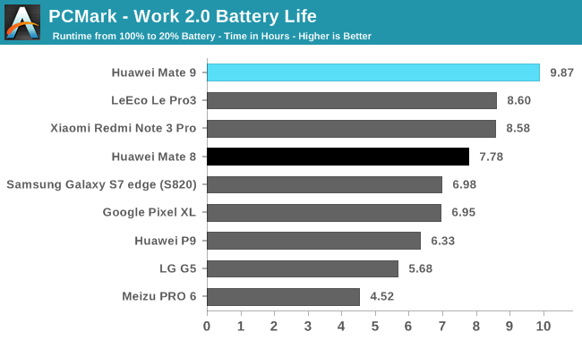
Despite the higher power consumption at the CPU’s highest operating points, Huawei’s Mate 9 actually does very well in our battery life tests. Its 13.25 hours of screen on time in our Wi-Fi Web Browsing test is a full 3 hours more than the Mate 8, and its nearly 10 hours in PCMark 2.0 is 27% better than the Mate 8. These real-world battery life results seem to be at odds with our CPU power measurements.
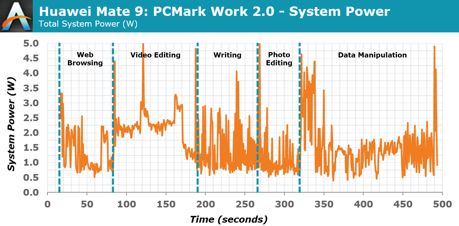
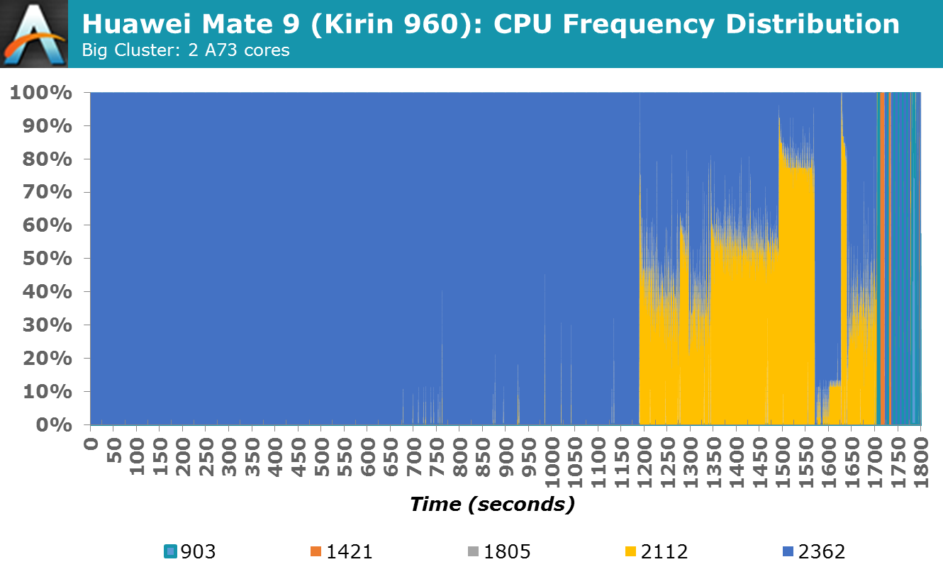
The graph above shows the Mate 9’s total system power consumption while running the PCMark 2.0 performance tests (all radios were turned off and the display’s brightness was calibrated to only 10 nits to better isolate the power consumption of the internal components). With the exception of some power spikes caused by increased activity while loading the next test, total power consumption remains below 3W and generally below 2W, well under the 5.3W we measured from Kirin 960’s four big cores.
I’m showing this graph because most of the apps we use everyday behave similarly to PCMark, where we see threads migrate from the little cores to the big cores and back again and DVFS working hard to match CPU frequency with load (actually, most apps would show significantly more CPU idle time, so PCMark is still a bit extreme in this regard). Many workloads will only use 1-2 big cores too, like we see here with PCMark. With only 2 cores at their max operating point, the Kirin 960 only consumes 754mW more power than Kirin 950 instead of 1601mW more when using 4 cores. So while CPU efficiency is certainly important, we need to frame it in terms of real-world workloads, and we also cannot forget the impact software (scheduler, CPUfreq, CPUidle) has on overall battery life.
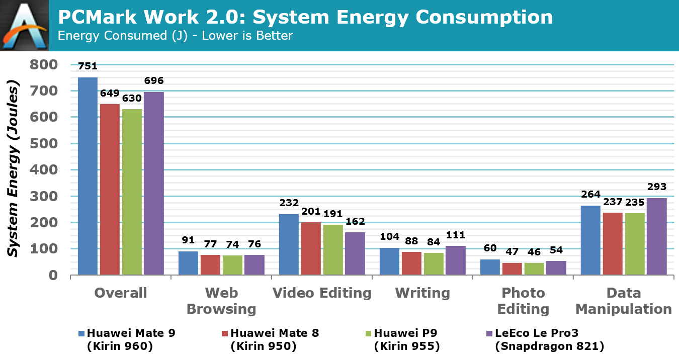
Looking at power alone can be misleading; a device may use more power than another, but if it completes the task in less time, it may actually use less energy, leading to longer battery life. For both of the graphs above, the phones’ radios were turned off and their displays calibrated to only 10 nits (the lowest common setting) to reduce the impact of different screen sizes and efficiencies from skewing the results.
In the first graph, which shows the total energy consumed by each phone when running the PCMark 2.0 performance tests, the Mate 9 consumes 16% more energy overall than the Mate 8 (despite my efforts to minimize display influence, the P9’s energy consumption is slightly lower than the Mate 8’s, which is likely because of its smaller screen). The Video and Photo Editing tests, which employ the GPU, show some of the biggest percent differences, but the Writing test, which makes frequent use of the CPU’s big cores, also shows a larger than average difference. The LeEco Le Pro3 and its Snapdragon 821 SoC actually consumes more energy than the Mate 9 in the Data Manipulation and Writing tests, where it has to use its 2 high-performance Kryo cores, but less in the Video and Photo Editing tests that use the GPU.
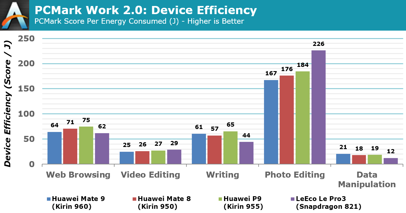
The second graph divides the PCMark score by the energy consumed to show efficiency. Because of the Mate 9’s better performance, it’s actually 7% more efficient than the Mate 8 in the Writing test and 17% more efficient in the Data Manipulation test. The Mate 9’s GPU efficiency is the worst of the group, judging by its scores in the Video and Photo Editing tests. In contrast, the Pro3’s Adreno 530 GPU posts the highest efficiency values in these tests.
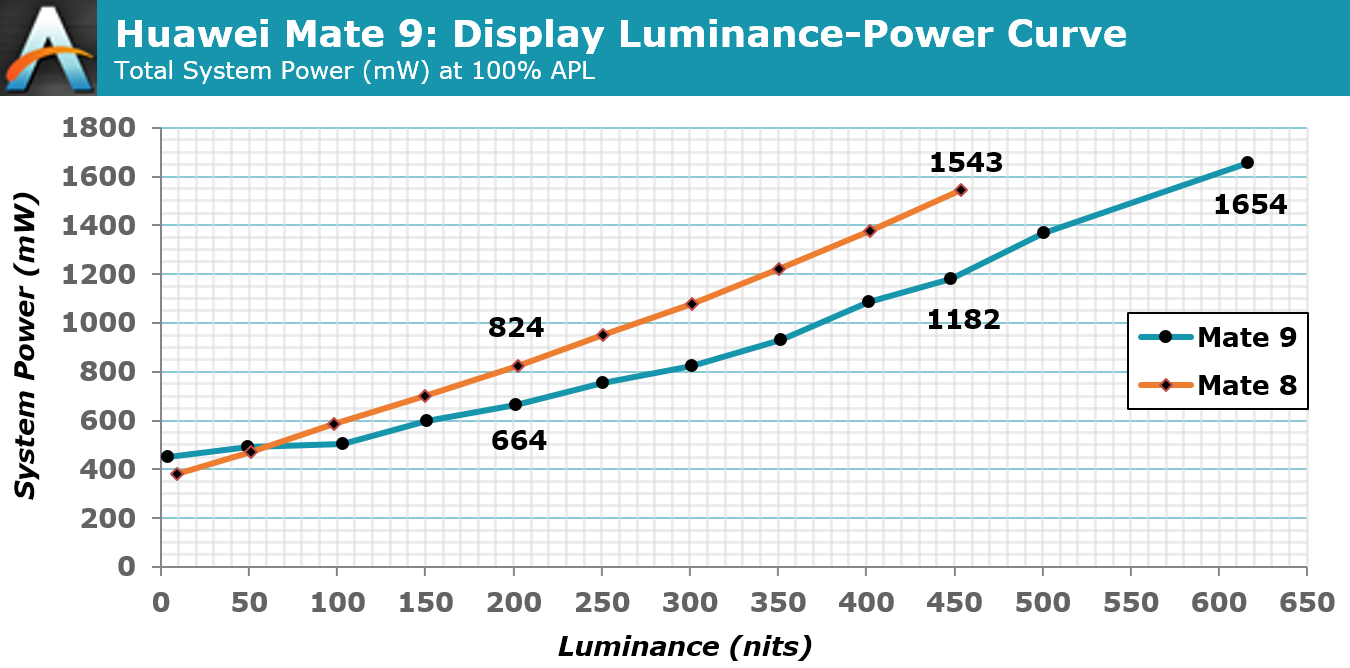
The Mate 9 lasts longer than the Mate 8 in the PCMark battery test despite its Kirin 960 SoC consuming more energy, so Huawei must have reduced energy consumption elsewhere to compensate. The display is the most obvious place to look, and the graph above clearly shows that the Mate 9’s display is more efficient. At 200 nits, the value we use for our battery tests, the Mate 9 shows an estimated 19% power reduction. In the time it takes to run PCMark, this translates to 82 J of energy, nearly erasing the 102 J difference between the Mate 9 and Mate 8. I suspect the difference in display power may actually be a little bigger, but I lack the equipment to make a more precise measurement. This still does not account for all of the Mate 9’s power savings, however, but a full accounting is beyond the scope of this article.
CPU Thermal Stability
Our CPU throttling test uses the same power virus we used above with two threads running on two of the big A73 CPU cores for a duration of about 30 minutes. The goal is to determine a device’s ability to sustain peak CPU performance without throttling and potentially reducing user experience. This is a product of CPU power consumption, the device’s ability to dissipate heat, and the device’s thermal safety limits.
The Mate 8 and its Kirin 950 are able to sustain peak performance with two A72 cores indefinitely, a remarkable feat. The Mate 9 does not fare as well because of Kirin 960’s elevated power use; however, it still manages to hold two of its A73 cores at peak frequency for 11.3 minutes and does not throttle enough to affect performance in a noticeable way for 20 minutes, which is still a very good result. I cannot think of any CPU-centric workloads for a phone that would load two big cores for anywhere near this long, so it’s safe to say that CPU throttling is not a problem for the Mate 9. It will be interesting to see if this holds true for Huawei’s smaller phones such as the P10, which will not be able to dissipate heat as readily as the big, aluminum Mate 9.


86 Comments
View All Comments
BedfordTim - Tuesday, March 14, 2017 - link
I suspect it comes down to cost and usage. The iPhone cores are roughly four times the size of an A73.name99 - Tuesday, March 14, 2017 - link
True. But the iPhone cores are still small ENOUGH. The main CPU complex on an A10 (two big cores, two small cores, and L2, is maybe 15 mm^2.ARM STILL seems to be optimizing for core area, and then spending that same core area anyway in octacores and decacores. It makes no sense to me.
Obviously part of it is that Apple must be throwing a huge number of engineers at the problem. But that's not enough; there has to be some truly incredible project management involved to keep all those different teams in sync, and I don't think anyone has a clue how they have done that.
They certainly don't seem to be suffering from any sort of "mythical man-month" Fred Brooks problems so far...
My personal suspicion is that, by luck or by hiring the best senior engineer in the world, they STARTED OFF at a place that is pretty much optimal for the trajectory they wanted.
They designed a good 3-wide core, then (as far as anyone can tell) converted that to a 6-wide core by clustering and (this is IMPORTANT) not worrying about all the naysayers who said that a very wide core could not be clocked very high.
Once they had the basic 6-wide core in place, they've had a superb platform on top of which different engineers can figure out improved sub-systems and just slot them in when ready. So we had the FP pipeline redesigned for lower latency, we had an extra NEON functional unit added, we've doubtless had constant improvements to branch prediction, I-fetching, pre-fetching, cache placement and replacement; and so on --- but these are all (more or less) "easy" to optimize given a good foundation on which to build.
I suspect, also, that unlike some in the industry, they have been extremely open to new ideas from academia, so that there's an implementation turnaround time of maybe two years or so from encountering a good idea (say a new design for a cluster predictor) through simulating it to validate its value, to implementing it.
I'm guessing that management (again unlike most companies) is willing to entertain a constant stream of ideas (from engineers, from reading the literature, from talking to academics) and to ACCEPT and NOT COMPLAIN about the cost of writing the simulations, in the full understanding that only 5 or 10% of simulated ideas are worth emulating. My guess is that they've managed to increase frequency rapidly (in spite of the 6-wide width) by implementing a constant stream of the various ideas that have been published (and generally mocked or ignored by the industry) for ways to scale things like load-store queues, issue, and rename --- the standard frequency/power pain-points in OoO design.
Meanwhile ARM seems to suffer from terminal effort-wasting. Apple has a great design, which they have been improving every year. ARM's response, meanwhile, has been to hop like a jack rabbit from A57 to A72 to A73, with no obvious conceptual progression. If each design spends time revising basics like the decoder and the optimal pipeline width, there's little time left to perform the huge number of experiments that I think Apple perform to keep honing the branch predictors, the instruction fusion, the pre-fetchers, and so on.
It reminds me of a piece of under-appreciated software, namely Mathematica, which started off with a ridiculously good foundation and horrible performance. But because the foundation was so good, every release had to waste very little time re-inventing the wheel, it could just keep adding and adding, until the result is just unbelievable.
Meteor2 - Wednesday, March 15, 2017 - link
Didn't Jim Keller have something to do with their current architecture?And yes, Apple seems to have excellent project management. Really, they have every stage of every process nailed. They're not the biggest company in the world by accident.
Meteor2 - Wednesday, March 15, 2017 - link
Also don't forget that (like Intel) ARM has multiple design teams. A72 and A73 are from separate teams; from that perspective, ARM's design progression does make sense. The original A73 'deepdive' by Andrei explained it very well.name99 - Wednesday, March 15, 2017 - link
This is a facet of what I said about project management.The issue is not WHY there are separate CPU design teams --- no-one outside the companies cares about the political compromises that landed up at that point.
The issue is --- are separate design teams and restarting each design from scratch a good fit to the modern CPU world?
It seems to me that the answer has been empirically answered as no, and that every company that follows this policy (which seem to include IBM, don't know about QC or the GPU design teams) really ought to rethink. We don't recreate compilers, or browsers, or OS's every few years from scratch, but we seem to have taken it for granted that doing so for CPUs made sense.
I'm not sure this hypothesis explains everything --- no-one outside Apple (and few inside) have the knowledge necessary to answer the question. But I do wonder if the biggest part of Apple's success came from their being a SW company, and thus looking at CPU design as a question of CONSTANTLY IMPROVING a good base, rather than as a question of re-inventing the wheel every few years the way the competition has always done things.
Meteor2 - Wednesday, March 15, 2017 - link
Part of having separate teams is to engender competition; another is to hedge bets and allow risk-taking. Core replacing Netburst is the standard example, I suppose. I'm sure there are others but they aren't coming to mind at the moment... Does replacing Windows CE with Windows 10 count?Meteor2 - Wednesday, March 15, 2017 - link
Methinks it's more to do with Safari having some serious optimisations for browser benchmarks baked in deep.I'd like to see the A10 subjected to GB4 and SpecInt.
name99 - Wednesday, March 15, 2017 - link
The A10 GeekBench numbers are hardly secret. Believe me, they won't make you happy.SPEC numbers, yeah, we're still waiting on those...
name99 - Wednesday, March 15, 2017 - link
Here's an example:https://browser.primatelabs.com/v4/cpu/959859
Summary:
Single-Core Score 3515
Crypto Score 2425
Integer Score 3876
Floating Point Score 3365
Memory Score 3199
The even briefer summary is that basically every sub-benchmark has A10 at 1.5x to 2x the Kirin 960 score. FP is even more brutal with some scores at 3x, and SGEMM at ~4.5x.
(And that's the A10... The A10X will likely be out within a month, likely fabbed on TSMC 10nm, likely an additional ~50% faster...)
Meteor2 - Wednesday, March 15, 2017 - link
Thanks. Would love to see those numbers in Anandtech charts, and normalised for power.