HiSilicon Kirin 960: A Closer Look at Performance and Power
by Matt Humrick on March 14, 2017 7:00 AM EST- Posted in
- Smartphones
- Mobile
- SoCs
- HiSilicon
- Cortex A73
- Kirin 960
Memory Performance
ARM made several improvements to the A73’s memory system. Both L1 caches see an increase in size, with the I-cache growing from 48KB (A72) to 64KB and the D-cache doubling in size to 64KB. The A73 includes several other changes, such as enhanced prefetching, that should improve cache performance too.
The A73 still has 2 AGUs like the A72, but they are now capable of both load and store operations instead of having each AGU dedicated to a single operation like in the A72, which should improve the issue rate into main system memory.
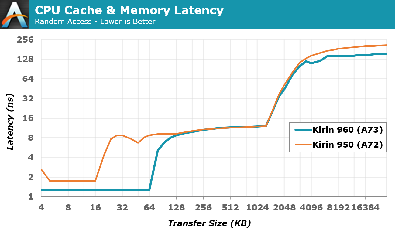
The Kirin 960’s larger 64KB L1 cache maintains a steady latency of 1.27ns versus 1.74ns for the Kirin 950, a 27% improvement that far exceeds the 2.6% difference in CPU frequency, highlighting the A73’s L1 cache improvements. L2 cache latency is essentially the same, but Kirin 960 again shows a 27% latency improvement over Kirin 950 when accessing main memory, which should be beneficial for the latency sensitive CPUs.
Memory bandwidth results are less definitive, however. The Kirin 960 shows up to a 30% improvement in L1 read bandwidth over the Kirin 950 depending on the access pattern used, although L1 write bandwidth is lower by nearly the same amount. The 960’s L2 cache bandwidth is also lower for both read and write by up to about 30%.
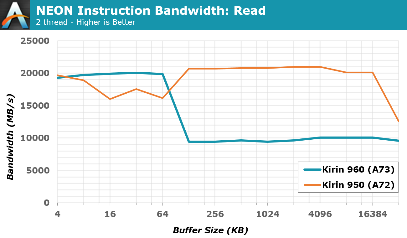
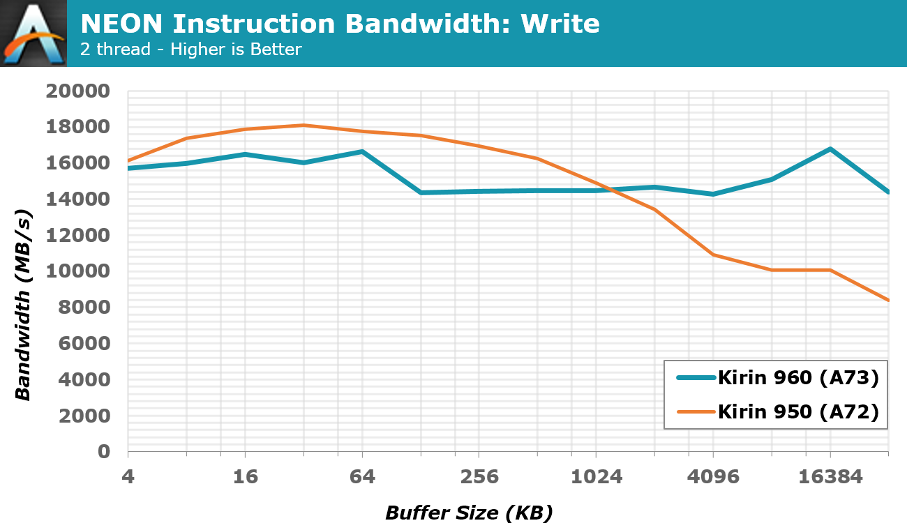
The two graphs above, which show reading and writing NEON instructions using two threads, help to illustrate Kirin 960’s memory bandwidth. When reading instructions, Kirin 960’s L1 cache outperforms the 950’s, but bandwidth drops once it hits the L2 cache. The Kirin 950 outpaces the 960 when writing to both L1 and L2, only falling below the 960’s bandwidth when writing to system memory. This reduction in cache bandwidth could help explain the Kirin 960’s performance regression in several of Geekbench 4’s floating-point tests.
| Geekbench 4 - Memory Performance Single Threaded |
||||
| Kirin 960 | Kirin 950 (% Advantage) |
Exynos 7420 (% Advantage) |
Snapdragon 821 (% Advantage) |
|
| Memory Copy | 4.55 GB/s | 3.67 GB/s (23.87%) |
3.61 GB/s (26.04%) |
7.82 GB/s (-41.84%) |
| Memory Latency | 12.1 Mops/s | 9.6 Mops/s (25.39%) |
5.6 Mops/s (115.67%) |
6.6 Mops/s (81.82%) |
| Memory Bandwidth | 15.5 GB/s | 9.2 GB/s (69.28%) |
7.5 GB/s (105.84%) |
13.5 GB/s (14.53%) |
While the Kirin 960’s L1/L2 cache performance is mixed, it holds a clear advantage over the Kirin 950 when using system memory. Memory latency improves by 25%, about the same amount our internal testing shows, and memory bandwidth improves by 69%. The A73’s two load/store AGUs are likely responsible for a large chunk of the additional memory bandwidth, with the Mate 9’s higher memory bus frequency helping some too.
System Performance
Now it’s time to see how Kirin 960’s lower-level CPU and memory results translate into real-world performance, keeping in mind that OEMs can influence the balance between performance and battery life in a number of ways, including adjusting thermal limits and parameters that govern CPU scheduler and DVFS behavior, which is one reason why two devices with the same SoC can perform differently.
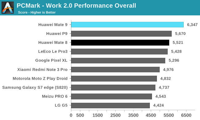
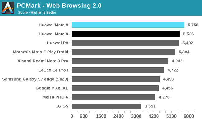
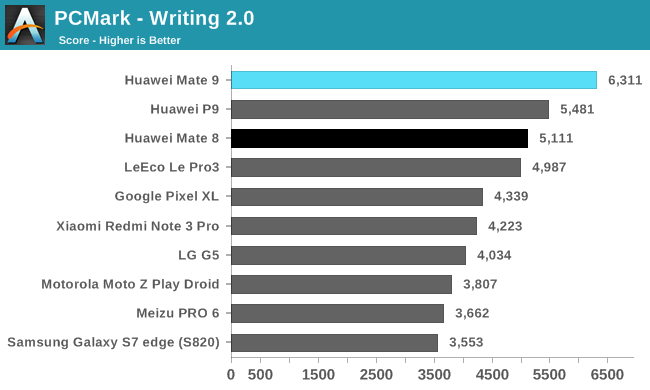
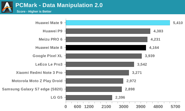
PCMark includes several realistic workloads that stress the CPU, GPU, RAM, and NAND storage using Android API calls many common apps use. The Mate 9 and its Kirin 960 SoC land at the top of each chart, outpacing the Mate 8 and its Kirin 950 by 15% overall and the top-performing Snapdragon 821 phones by up to 20%.
The Mate 9’s advantage over the Mate 8 is only 4% in the Web Browsing test, but it’s still the fastest phone we’ve tested so far. Integer performance is not the Kryo CPU’s strength, and in this integer-heavy test all of the Snapdragon 820/821 phones fall behind SoCs using ARM’s A72 and A73 CPUs, with LeEco’s Le Pro3, the highest performing Snapdragon 821 phone, finishing 18% slower than the Mate 9.
The Writing test performs a variety of operations, including PDF processing and file encryption (both integer workloads), along with some memory operations and even reading and writing some files to internal NAND, and it tends to generate frequent, short bursts of activity on the big CPU cores. This seems to suit the Mate 9 just fine, because it extends its performance advantage over the Mate 8 to 23%. There’s a pretty big spread between the Snapdragon 820/821 phones; the LeEco Le Pro3, the best performer in the family, is 40% faster than the Galaxy S7 edge, a prime example of how other hardware components and OEM software tinkering can affect the overall user experience.
The Data Manipulation test is another primarily integer workload that measures how long it takes to parse chunks of data from several different file types and then records the frame rate while interacting with dynamic charts. In this test, the Mate 9 is 30% faster than the Mate 8 and 37% faster than the Pixel XL.
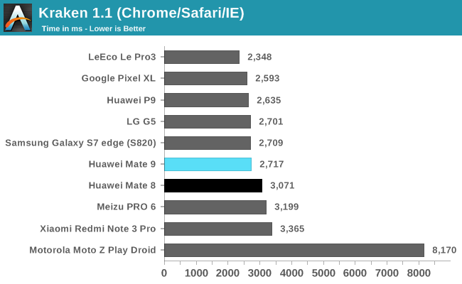
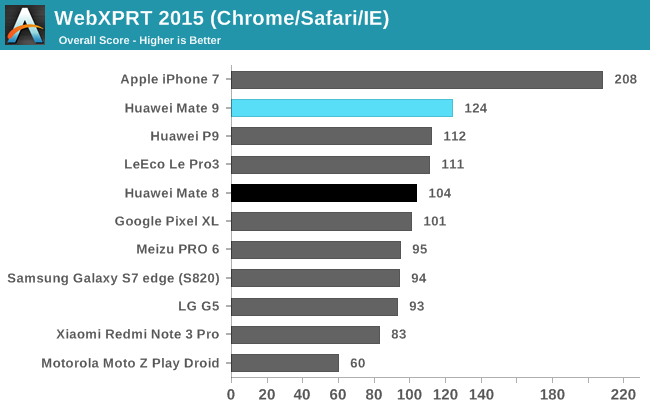
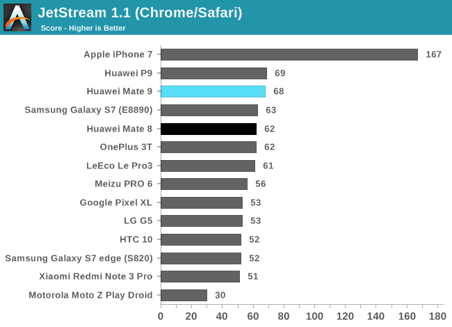
All of the Snapdragon 820/821 phones perform well in the Kraken JavaScript test, pulling ahead of the Mate 9 by a small margin. The P9 uses Kirin 955’s 7% CPU frequency advantage to help it keep up with the Mate 9 in Kraken and JetStream. The Mate 9 still pulls ahead by 11% in WebXPRT 2015, though, and outperforms the Mate 8 by 10% to 19% in all three tests. The Moto Z Play Droid, the only phone in the charts to use an octa-core A53 CPU configuration, cannot even manage half the performance of the Mate 9, which is similar to what our integer IPC tests show.
The Kirin 960 showed mixed results in our lower-level CPU and memory testing, pulling ahead of the Kirin 950 in some areas while falling behind in others. But when looking at system level tests using real-world workloads, the Mate 9 and its Kirin 960 are the clear winners. There are many hardware and software layers between you and the SoC, which is why it’s important not to use an SoC benchmark to test system performance and a system benchmark, such as PCMark, to test CPU performance.


86 Comments
View All Comments
BedfordTim - Tuesday, March 14, 2017 - link
I suspect it comes down to cost and usage. The iPhone cores are roughly four times the size of an A73.name99 - Tuesday, March 14, 2017 - link
True. But the iPhone cores are still small ENOUGH. The main CPU complex on an A10 (two big cores, two small cores, and L2, is maybe 15 mm^2.ARM STILL seems to be optimizing for core area, and then spending that same core area anyway in octacores and decacores. It makes no sense to me.
Obviously part of it is that Apple must be throwing a huge number of engineers at the problem. But that's not enough; there has to be some truly incredible project management involved to keep all those different teams in sync, and I don't think anyone has a clue how they have done that.
They certainly don't seem to be suffering from any sort of "mythical man-month" Fred Brooks problems so far...
My personal suspicion is that, by luck or by hiring the best senior engineer in the world, they STARTED OFF at a place that is pretty much optimal for the trajectory they wanted.
They designed a good 3-wide core, then (as far as anyone can tell) converted that to a 6-wide core by clustering and (this is IMPORTANT) not worrying about all the naysayers who said that a very wide core could not be clocked very high.
Once they had the basic 6-wide core in place, they've had a superb platform on top of which different engineers can figure out improved sub-systems and just slot them in when ready. So we had the FP pipeline redesigned for lower latency, we had an extra NEON functional unit added, we've doubtless had constant improvements to branch prediction, I-fetching, pre-fetching, cache placement and replacement; and so on --- but these are all (more or less) "easy" to optimize given a good foundation on which to build.
I suspect, also, that unlike some in the industry, they have been extremely open to new ideas from academia, so that there's an implementation turnaround time of maybe two years or so from encountering a good idea (say a new design for a cluster predictor) through simulating it to validate its value, to implementing it.
I'm guessing that management (again unlike most companies) is willing to entertain a constant stream of ideas (from engineers, from reading the literature, from talking to academics) and to ACCEPT and NOT COMPLAIN about the cost of writing the simulations, in the full understanding that only 5 or 10% of simulated ideas are worth emulating. My guess is that they've managed to increase frequency rapidly (in spite of the 6-wide width) by implementing a constant stream of the various ideas that have been published (and generally mocked or ignored by the industry) for ways to scale things like load-store queues, issue, and rename --- the standard frequency/power pain-points in OoO design.
Meanwhile ARM seems to suffer from terminal effort-wasting. Apple has a great design, which they have been improving every year. ARM's response, meanwhile, has been to hop like a jack rabbit from A57 to A72 to A73, with no obvious conceptual progression. If each design spends time revising basics like the decoder and the optimal pipeline width, there's little time left to perform the huge number of experiments that I think Apple perform to keep honing the branch predictors, the instruction fusion, the pre-fetchers, and so on.
It reminds me of a piece of under-appreciated software, namely Mathematica, which started off with a ridiculously good foundation and horrible performance. But because the foundation was so good, every release had to waste very little time re-inventing the wheel, it could just keep adding and adding, until the result is just unbelievable.
Meteor2 - Wednesday, March 15, 2017 - link
Didn't Jim Keller have something to do with their current architecture?And yes, Apple seems to have excellent project management. Really, they have every stage of every process nailed. They're not the biggest company in the world by accident.
Meteor2 - Wednesday, March 15, 2017 - link
Also don't forget that (like Intel) ARM has multiple design teams. A72 and A73 are from separate teams; from that perspective, ARM's design progression does make sense. The original A73 'deepdive' by Andrei explained it very well.name99 - Wednesday, March 15, 2017 - link
This is a facet of what I said about project management.The issue is not WHY there are separate CPU design teams --- no-one outside the companies cares about the political compromises that landed up at that point.
The issue is --- are separate design teams and restarting each design from scratch a good fit to the modern CPU world?
It seems to me that the answer has been empirically answered as no, and that every company that follows this policy (which seem to include IBM, don't know about QC or the GPU design teams) really ought to rethink. We don't recreate compilers, or browsers, or OS's every few years from scratch, but we seem to have taken it for granted that doing so for CPUs made sense.
I'm not sure this hypothesis explains everything --- no-one outside Apple (and few inside) have the knowledge necessary to answer the question. But I do wonder if the biggest part of Apple's success came from their being a SW company, and thus looking at CPU design as a question of CONSTANTLY IMPROVING a good base, rather than as a question of re-inventing the wheel every few years the way the competition has always done things.
Meteor2 - Wednesday, March 15, 2017 - link
Part of having separate teams is to engender competition; another is to hedge bets and allow risk-taking. Core replacing Netburst is the standard example, I suppose. I'm sure there are others but they aren't coming to mind at the moment... Does replacing Windows CE with Windows 10 count?Meteor2 - Wednesday, March 15, 2017 - link
Methinks it's more to do with Safari having some serious optimisations for browser benchmarks baked in deep.I'd like to see the A10 subjected to GB4 and SpecInt.
name99 - Wednesday, March 15, 2017 - link
The A10 GeekBench numbers are hardly secret. Believe me, they won't make you happy.SPEC numbers, yeah, we're still waiting on those...
name99 - Wednesday, March 15, 2017 - link
Here's an example:https://browser.primatelabs.com/v4/cpu/959859
Summary:
Single-Core Score 3515
Crypto Score 2425
Integer Score 3876
Floating Point Score 3365
Memory Score 3199
The even briefer summary is that basically every sub-benchmark has A10 at 1.5x to 2x the Kirin 960 score. FP is even more brutal with some scores at 3x, and SGEMM at ~4.5x.
(And that's the A10... The A10X will likely be out within a month, likely fabbed on TSMC 10nm, likely an additional ~50% faster...)
Meteor2 - Wednesday, March 15, 2017 - link
Thanks. Would love to see those numbers in Anandtech charts, and normalised for power.