HiSilicon Kirin 960: A Closer Look at Performance and Power
by Matt Humrick on March 14, 2017 7:00 AM EST- Posted in
- Smartphones
- Mobile
- SoCs
- HiSilicon
- Cortex A73
- Kirin 960
HiSilicon’s Kirin 950 proved to be a breakout product for the Huawei subsidiary, ultimately finding a home in many of Huawei’s flagship phones, including the Mate 8, P9, P9 Plus, and Honor 8. Its big.LITTLE combination of four A72 and four A53 CPU cores manufactured on TSMC’s 16nm FF+ FinFET process delivered excellent performance and efficiency. Somewhat surprisingly, it turned out to be one of the best, if not the best, implementation of ARM’s IP we’ve seen.
Because of the 950’s success, we were eager to see what improvements the Kirin 960 could offer. In our review of the Huawei Mate 9, the first device to use the new SoC, we saw gains in most of our performance and battery life tests relative to the Mate 8 and its Kirin 950 SoC. Now it’s time to dive a little deeper and answer some of our remaining questions: How does IPC compare between the A73, A72, and other CPU cores? How is memory performance impacted by the A73’s microarchitecture changes? Does CPU efficiency improve? How much more power do the extra GPU cores consume?
| HiSilicon High-End Kirin SoC Lineup | |||
| SoC | Kirin 960 | Kirin 955 | Kirin 950 |
| CPU | 4x Cortex-A73 @ 2.36GHz 4x Cortex-A53 @ 1.84GHz |
4x Cortex-A72 @ 2.52GHz 4x Cortex-A53 @ 1.81GHz |
4x Cortex-A72 @ 2.30GHz 4x Cortex-A53 @ 1.81GHz |
| GPU | ARM Mali-G71MP8 1037MHz |
ARM Mali-T880MP4 900MHz |
|
| Memory | 2x 32-bit LPDDR4 @ 1866MHz 29.9GB/s |
2x 32-bit LPDDR3 @ 933MHz (14.9GB/s) or 2x 32-bit LPDDR4 @ 1333MHz (21.3GB/s) (hybrid controller) |
|
| Interconnect | ARM CCI-550 | ARM CCI-400 | |
| Storage | UFS 2.1 | eMMC 5.0 | |
| ISP/Camera | Dual 14-bit ISP (Improved) |
Dual 14-bit ISP 940MP/s |
|
| Encode/Decode | 2160p30 HEVC & H.264 Decode & Encode 2160p60 HEVC Decode |
1080p H.264 Decode & Encode 2160p30 HEVC Decode |
|
| Integrated Modem | Kirin 960 Integrated LTE (Category 12/13) DL = 600Mbps 4x20MHz CA, 64-QAM UL = 150Mbps 2x20MHz CA, 64-QAM |
Balong Integrated LTE (Category 6) DL = 300Mbps 2x20MHz CA, 64-QAM UL = 50Mbps 1x20MHz CA, 16-QAM |
|
| Sensor Hub | i6 | i5 | |
| Mfc. Process | TSMC 16nm FFC | TSMC 16nm FF+ | |
The Kirin 960 is the first SoC to use ARM’s latest A73 CPU cores, which seems fitting considering the Kirin 950 was the first to use ARM’s A72. Its CPU core frequencies see a negligible increase relative to the Kirin 950: 1.81GHz to 1.84GHz for the four A53s and 2.30GHz to 2.36GHz for the four A73s. Setting the peak operating point for the A73 cores lower than the 2.52GHz used by Kirin 955’s A72 cores, and lower still than the 2.8GHz that ARM targets for 16nm, is an interesting and deliberate choice by HiSilicon to limit the CPU’s power envelope, allowing the bigger GPU to take a larger chunk.
We’ve already discussed the A73’s microarchitecture in depth, so I’ll just summarize a few of the highlights. For starters, the A73 stems from the A17 and does not belong to the A15/A57/A72 Austin family tree. This means the differences between the A72 and A73 are more substantial than the small change in product numbering would suggest, particularly in the CPU’s front end.
The biggest difference is a reduction in decoder width, which is now 2-wide instead of 3-wide like the A72. This sounds like a downgrade on paper; however, there’s likely some workloads where the A72’s instruction fetch block fails to consistently saturate the decoder, so the actual performance impact of the A73’s narrower decode stage may not be that severe.
In many cases, instruction dispatch throughput should actually improve relative to the A72. The A73’s shorter pipeline reduces front-end latency, including 1-2 fewer cycles for the decoder, which can decode most instructions in a single cycle, and 1 less cycle for the fetch stage. The L1 instruction cache doubles in size and is optimized for better throughput, and changes to the instruction fetch block reduce instruction bubbles. ARM also says the A73 includes a new, more accurate branch predictor, with a larger BTAC (Branch Target Address Cache) structure and a new 64-entry “micro-BTAC” for accelerating branch prediction.
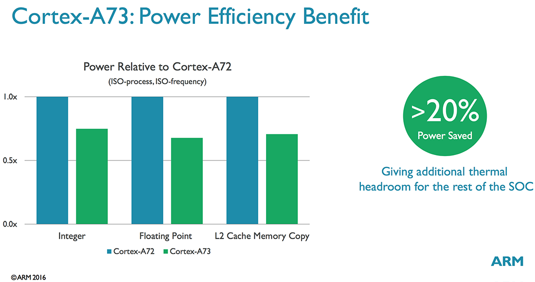
There are several other changes to the front end too, not to mention further along the pipeline, but it should be obvious by now that the A73 is a very different beast than the A72, grown from a different design philosophy. While the Austin family (A72) targeted industrial and low-power server applications in addition to mobile, the A73 focuses specifically on mobile, where power and area become an even higher priority. ARM says the A73 consumes 20%-30% less power than the A72 (same process, same frequency) and is up to 25% smaller (same process, same performance targets).
When it comes to Kirin 960’s GPU, however, HiSilicon is clearly chasing performance instead of efficiency. With its previous SoCs, the Kirin 950/955 in particular, HiSilicon was criticized for using four-core Mali configurations while Samsung packed in eight or twelve Mali cores in its Exynos SoCs and Qualcomm squeezed more ALU resources into its Adreno GPUs. This was not entirely justified, though, because the Kirin 950’s Mali-T880MP4 GPU was capable of playing nearly any game available at acceptable frame rates and the performance difference between the Mate 8 (Kirin 950), Samsung Galaxy S7 edge (Snapdragon 820), and Galaxy S7 (Exynos 8890) after reaching thermal equilibrium is minimal.
Whether in response to this criticism or to enable future use cases such as VR/AR, HiSilicon has significantly increased the Kirin 960’s peak GPU performance. Not only is it the first to use ARM’s latest Mali-G71 GPU, but it doubles core count to eight and boosts the peak frequency to 1037MHz, 15% higher than the 950’s smaller GPU.
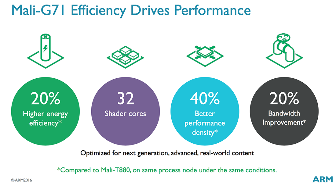
The Mali-G71 uses ARM’s new Bifrost microarchitecture, which moves from an SIMD ISA that relied on Instruction Level Parallelism (ILP) to a scalar ISA designed to take advantage of Thread Level Parallelism (TLP) like modern desktop GPU architectures from Nvidia and AMD. I’m not going to explain the difference in depth here, but basically this change allows better utilization of the shader cores, increasing throughput and performance. ARM’s previous Midgard microarchitecture needed to extract 4 instructions from a single thread and execute them concurrently to achieve full utilization of a single shader core, which is not easy to do consistently. In contrast, Bifrost can group 4 separate threads together on a shader core and execute a single instruction from each one, which is more inline with modern graphics and compute workloads.
Now that we have a better understanding for Kirin 960’s design goals—better efficiency for the CPU and higher peak performance for the GPU—and a summary of the hardware changes HiSilicon made to achieve them, we’re ready to see how the performance and power consumption of the Kirin 960 compares to the 950/955 and other recent SoCs.


86 Comments
View All Comments
lilmoe - Tuesday, March 14, 2017 - link
I read things thoroughly before criticizing. You should do the same before jumping in to support an idiotic comment like fanofanand's. He's more interested in insulting people than finding the truth.These tests are the ones which aren't working. No one gets nearly as much battery life as they report. Nor are the performance gains anywhere near what benchmarks like geekbench are reporting. If something isn't working, one should really look for other means. That's how progress works.
You can't test a phone the same way you test a workstation. You just can't. NO ONE leaves their phone lying on a desk for hours waiting on it to finish compiling 500K lines of code, or rendering a one-hour 3D project or a 4K video file for their channel on Youtube. But they do spend a lot of time watching video on Youtube, browsing the web with 30 second pauses between each scroll, and uploading photos/videos to social media after applying filters. Where are these tests??? You know, the ones that actually MATTER for most people? You know, the ones that ST performance matters less for, etc, etc...
Anyway, I did suggest what I believe is a better, more realistic, method for testing. Hint, it's in the fifth paragraph of my original reply. But who cares right? We just want to know "which is the fastest", which method confirms our biases, regardless of the means of how such performance is achieved. Who cares about the truth.
People are stubborn. I get that. I'm stubborn too. But there's a limit at how stubborn people can be, and they need to be called out for it.
Meteor2 - Wednesday, March 15, 2017 - link
I'm with fanof and close on this one. Here we have a consistent battery of repeatable tests. They're not perfectly 'real-world' but they're not far off either; there's only so many things a CPU can do.I like this test suite (though I'd like to see GB/clock and SPi and GB/power calculated and graphed too). If you can propose a better one, do so.
close - Wednesday, March 15, 2017 - link
This isn't about supporting someone's comment, I was very clear which part I agree with: the one where you help come up with a practical implementation of your suggestion.Phone can and should be tested like normal desktops since the vast majority of them spend most of their time idling, just like phones. The next this is running Office like applications, normal browsing, and media consumption.
You're saying that "NO ONE leaves their phone lying on a desk for hours waiting on it to finish compiling 500K lines of code". But how many people would find even that relevant? How many people compile 500K lines of code regularly? Or render hours of 4K video? And I'm talking about percentage of the total.
Actually the ideal case for testing any device is multiple scenarios that would cover a more user types: from light browsing and a handful of phone calls to heavy gaming or media consumption. These all result in vastly different results as a SoC/phone might be optimized for sporadic light use or heavier use for example. So a phone that has best battery life and efficiency while gaming won't do so while browsing. So just like benchmarks, any result would only be valid for people who follow the test scenario closely in their daily routine.
But the point wasn't whether an actual "real world" type scenario is better, rather how exactly do you apply that real world testing into a sequence of steps that can be reproduced for every phone consistently? How do you make sure that all phones are tested "equally" with that scenario and that none has an unfair (dis)advantage from the testing methodology? Like Snapchat or FB being busier one day and burning through the battery faster.
Just like the other guy was more interested in insults (according to you), you seem more interested in cheap sarcasm than in actually providing an answer. I asked for a clear methodology. You basically said that "it would be great if we had world peace and end hunger". Great for a beauty pageant, not so great when you were asked for a testing methodology. A one liner is not enough for this. A methodology is you describing exactly how you proceed with testing the phones, step by step, while guaranteeing reproducibility and fairness. Also please explain how opening a browser, FB, or Snapchat is relevant for people who play games 2 hours per day, watch movies or actually use the phone as a phone and talk to other people.
You're making this more difficult than it should be. You look like you had plenty of time to think about this. I hald half a day and already I came up with a better proposal then yours (multiple scenarios vs. single scenario). And of course, I will also leave out the exact methodology part because this is a comment competition not an actual search for solutions.
lilmoe - Wednesday, March 15, 2017 - link
I like people who actually spend some time to reply. But, again, I'd appreciate it more if you read my comments more carefully. I told you that the answer you seek is in my first reply, in the fifth paragraph. If you believe I have "plenty of time" just for "cheap sarcasm", then sure we can end it here. If you don't, then go on reading.I actually like this website. That's why I go out of my way to provide constructive criticism. If I was simply here for trolling, my comments won't be nearly as long.
SoCs don't live in a vacuum, they come bundled with other hardware and software (Screen, radios, OS/Kernel), optimized to work on the device being reviewed. In the smartphone world, you can't come to a concrete conclusion on the absolute efficiency of a certain SoC based on one device, because many devices with the same SoC can be configured to run that SoC differently. This isn't like benchmarking a Windows PC, where the kernel and governer are fixed across hardware, and screens are interchangeable.
Authors keep acknowledging this fact, yet do very little to go about testing these devices using other means. It's making it hard for everyone to understand the actual performance of said devices, or the real bang for the buck they provide. I think we can agree on that.
"You're making this more difficult than it should be"
No, really, I'm not. You are. When someone is suggesting something a bit different, but everyone is slamming them for the sake of "convention" and "familiarity", then how are we supposed to make progress?
I'm NOT saying that one should throw benchmarks out. But I do believe that benchmarks should stay in meaningful context. They give you a rough idea about the snappiness of a ultra-mobile device, since it's been proven time after time that the absolute performance of these processors is ONLY needed for VERY short bursts, unlike workstations. However, they DO NOT give you anywhere near a valid representation of average power draw and device battery life, and neither do scripts written to run synthetic/artificial workloads. Period.
This is my point. I believe the best way to measure a specific configuration is by first specifying the performance point a particular OEM is targeting, and then measuring the power draw of that target. This comes in as the average clocks the CPU/GPU at various workloads, from gaming, browsing, playing video, to social media. It doesn't matter how "busy" these content providers are at specific times, the average clocks will be the same regardless because the workload IS the same.
I have reason to believe that OEMs are optimizing their kernels/governers for each app alone. Just like they did with benchmarks several years ago, where they ramp clocks up when they detect a benchmark running. Except, they're doing it the right way now, and optmizing specific apps to run differently on the device to provide the user with the best experience.
When you've figured out the average the OEM is targetting for various workloads, you'd certainly know how much power it's drawing, and how much battery life to expect AFTER you've already isolated other factors, such as the screen and radios. It also makes for a really nice read, as a bonus (hence, "worth investigating").
This review leaves an important question unanswered about this SoC's design (I'm really interested to know the answer); did HiSilicon cheap out on the fab process to make more money and leach on the success of its predecessor? Or did they do that with good intentions to optimize their SoC further for modern, real world workloads that currently used benchmarks are not detecting? I simply provided a suggest to answer that question. Does that warrant the language in his, or your reply? Hence my sarcasm.
fanofanand - Tuesday, March 14, 2017 - link
It's exciting to see the envelope being pushed, and though these are some interesting results I like that they are pushing forward and not with a decacore. The G71 looks like a botched implementation if it's guzzling power that heavily, I wonder if some firmware/software could fix that? A73 still looks awesome, and I can't wait to see a better implementation!psychobriggsy - Tuesday, March 14, 2017 - link
TBH the issue with the GPU appears to be down to the clock speed it is configured with.It's clear that this is set for benchmarking purposes, and it's good that this has been caught.
Once the GPU settles down into a more optimal 533MHz configuration, power consumption goes down significantly. Sadly it looks like there are four clock settings for the GPU, and they've wasted three of them on stupid high clocks. A better setup looks to be 800MHz, 666MHz, 533MHz and a power saving 400MHz that most Android games would still find overkill.
Meteor2 - Wednesday, March 15, 2017 - link
Performance/Watt is frankly rubbish whatever the clock speed. Clearly they ran out of time or money to implement Bifrost properly.fanofanand - Wednesday, March 15, 2017 - link
That's what I'm thinking, I read the preview to Bitfrost and thought "wow this thing is going to be killer!" I was right on the money, except that it's a killer of batteries, not competing GPUs.Shadowmaster625 - Tuesday, March 14, 2017 - link
What is HTML5 DOM doing that wrecks the Snapdragon 821 so badly?joms_us - Tuesday, March 14, 2017 - link
Just some worthless test that the Monkey devs put to show how awesome iPhones are. But if you do real side-by-side website comparison between iPhone and and phone with SD821, SD821 will wipe the floor.